This is the first version of the DeepDrive project, an STM32-Based ESC PCB Designed For Evaluating Motor Control Algorithms for BLDC (Brushless DC Motors). I’ve designed this board to be a development board that can be used to test various motor control algorithms, especially Sensorless FOC (Field-Oriented Control) with STM32.
In this article, I’ll show you the STM32 ESC PCB & schematic design steps, explain some of the design decisions that I’ve made, how to prepare the files needed for manufacturing, and how to place the PCB SMT order at JLCPCB who are kindly sponsoring this project as well.
This Project is Sponsored By JLCPCB

Table of Contents
- DeepDrive v1.0 ESC PCBA Overview
- STM32 ESC PCB Design Requirements
- DeepDrive v1.0 STM32 ESC Hardware HLD
- STM32 ESC Schematic Design Diagram
- STM32 ESC PCB Layout & Routing
- Placing PCBA Order @ JLCPCB
- STM32 ESC PCB Spinning a BLDC Motor
- Conclusion & Next Steps
- DeepDrive STM32 ESC PCB Project Video
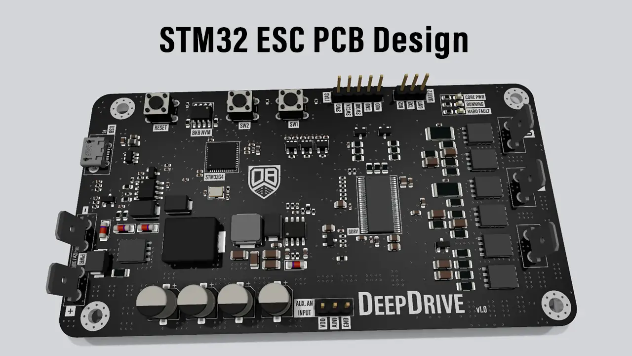
DeepDrive v1.0 ESC PCBA Overview
The intention behind this project was to create a customized ESC board for BLDC/PMSM motor control algorithm evaluation. I wanted some sort of motor control dev board that helps me demonstrate motor control algorithms and commutation schemes. Topics like six-step commutation, SPWM, SVPWM, and most importantly FOC (field-oriented control).
That led me to write down the complete requirements list of this project and start planning the HLD (High-Level Design). That consists of a lot of smaller pieces (blocks) of hardware that I did design, simulate, and test one by one afterward.
The whole thing was ready for fabrication back in early 2020 when the COVID-19 silicon shortage crisis disrupted the global market. So I had to abandon it till now in 2023 when JLCPCB kindly offered to sponsor the project and bring it to life again. FYI, during the silicon shortage crisis, the gate driver that I’m using was being sold for around 37US$/part, while it’s now 3US$/part. This is just one simple example of how the situation was back then.
The final project is shown below in KiCAD 3D viewer and in real life after fabrication and SMT assembly by JLCPCB. It’s really amazing how similar they look at the end.

STM32 ESC PCB Design Requirements
Here are the requirements of this project that I’ve listed down in the following categories before starting to design or select any part of the BOM.
Power Requirements
- 12VDC input & Handle up to 30A continuous (360W)
- RPP (Reverse Polarity Protection) + TVS For The DC Input
- Bulk Capacitors Bank For The DC-Link Voltage
- 3.3V DC-DC Buck Converter (Logic Supply)
- Power Logic Supply Over USB if No DC Input Exists
Gate Driver & Inverter Requirements
- 3-Phase Half-Bridge Smart Gate Driver
- 3-Phase Inverter That Consists of 6x MOSFETs (Low Rdson, High Id)
Measurements For Motor Control
- Dual-Shunt Phase Current Measurement
- DC-Link Voltage & Battery Voltage Measurement
- DC Current (Battery Current) Measurement
- Inverter Bridge Temperature Measurement
- 3-Phase Voltages Measurement
- 3-Phase BEMF Zero-Crossing Detection
Microcontroller & Auxiliaries
- STM32G4 Motor Control Microcontroller
- USB 2.0 Full Speed (Data Transfer to GUI on PC)
- Onboard Buttons & Indicator LEDs
- NVM (8kB I2C EEPROM)
- Aux. UART Port
- Aux. ADC Input
DeepDrive v1.0 STM32 ESC Hardware HLD
At this stage, we can easily come up with a first draft for the whole system’s HLD (High-Level Design) that indicates the system’s hardware design breakdown for smaller HW blocks and their interfaces. This will facilitate the process of design and BOM selection.
Vital components can also be selected by the end of the HLD draft. After we’ve decided on the number of hardware interfaces needed (ADC channels, UARTs, IO pins, etc). So we can select the microcontroller part more specifically and also the smart gate driver & inverter bridge’s MOSFETs.
The BOM selection process will still be ongoing but it starts here at the HLD stage and will continue until the end of the footprints assignment, where we’ll be ready to start the PCB layout and routing. Before starting the PCB layout and routing, the BOM selection process must be complete and pretty much stable. Any change in the BOM afterward will take more time to accommodate going back and forth from PCB<->Schematic.
Here is the HLD of the DeepDrive v1.0 project.

Note That this may look like a UML (unified modeling language) diagram but it actually isn’t. It’s my way to communicate HW HLD and you’re pretty much free to draw it however you like as long as it’s understandable by other engineers in your team.
STM32 ESC Schematic Design Diagram
Let’s now move to the most interesting part of the project, which is designing the circuits needed to complete the HLD (high-level design). We’ll go through the HW blocks mentioned in the HLD one at a time and discuss how to implement them and justify the design decisions that I’ve made during the design process.
For a more in-depth demonstration, it’s highly recommended to check out the project’s YouTube video as I go through the design decisions that I’ve made in this project with a bit more elaboration and explanation.
1. DC PWR In + RPP (Reverse Polarity Protection)
Here is the DC voltage input section of the ESC schematic design. There is a TVS diode that kicks in whenever the voltage goes beyond 30v, despite the fact that our input port is 12VDC. This is because the ESC will be switching an inductive load (BLDC/PMSM motor), so it’s expected to dump energy back into the supply while breaking or in fault conditions.

An inductor is also present on the DC input line for that purpose, to resist the back energy from the motor to protect my uni-directional power supply (regenerative breaking is not supported in this ESC design). The inductor helps also in reducing inrush current during power up that happens due to the large DC-Link voltage capacitors bank.
RPP is achieved by using an N-Channel MOSFET in the GND path. The MOSFETs gate is protected with zener diodes (Vz=16.8v extended part in JLCPCB library). I could have used a P-Channel MOSFET in the +ve rail path instead both options are totally fine, it’s up to you to decide which path to go.
2. Logic Supply (DC-DC Buck Converter)
We need to step down the 12v DC input voltage to 3.3v in order to supply the STM32 core as well as various logic elements and measurement circuits across the board. Supporting up to 4.5A is definitely overkill compared to the actual needs of the project, this will be optimized in the upcoming revision of the board.

An LDO could have been used instead to reduce the BOM cost significantly and the switching noise of the buck converter. However, stepping down a 12VDC to 3.3v will generate a significant power loss (heat).
3. Gate Driver + 3PH Inverter Bridge + RC Snubbers
I’ve decided to go for a Ti DRV8302 smart gate driver which I’ve been using in other designs and motor control ECUs. It costs only 3US$ in the JLCPCB parts library, which is a very good value for money as far as I know.
The DRV8302 gives us the basic hardware fault detection that we’d expect from a smart gate driver as well as internal 2x current sensing op-amps with Vref/2 offset voltage built-in. It’s got a HW programmable deadtime, overcurrent detection, and op-amp gain. It’s also a built-in buck converter that I could have used instead of what I’ve built earlier but I’ll do this optimization in the next revision I believe.

You can definitely use 3x simple half-bridge gate drivers like the well-known IR2110. It’ll cost you around 1US$/part which means you’re already at the same price point as a DRV8302 chip while you’re still missing current sensing amps, current offset circuitry, smart gate driver fault detection, and more other features.
At the OPS (output stage) of each inverter leg, you’ll find a couple of RC networks. Those are called snubber circuits that we typically use to protect the output drivers (MOSFETs) from the inductive spikes that stem from switching an inductive load (Motors).
The RC Snubber circuits limit the inductive voltage spikes that the inverter’s MOSFETs experience while switching. The IRF7440 MOSFETs are rated for a maximum VDS of 40v, so we need to make sure that it doesn’t experience a higher voltage than this during operation.
4. Phase Current Measurement (Dual Shunt)
For the 3-phase current measurement, I’ve decided to go for a dual shunt configuration. It’s very easy to implement in software and it doesn’t cost very much in terms of hardware needed. Here is a summarized comparison between all 3 different configurations that you may encounter while studying this subject.
Triple Shunt: This is obviously the most expensive solution among all while being the easiest to implement in software. The third shunt resistor is actually redundant if you’re going to code the current reconstruction equation by yourself as I’ll demonstrate hereafter in the dual shunt method.
Dual Shunt: This is the most balanced option among all in terms of cost and ease of implementation in software. You can easily read 2x phase currents using the dual shunt configuration and reconstruct the third phase current using the equation ( iU + iV + iW = 0 ).
Single Shunt: This is obviously the cheapest solution of all. However, it’s way more complex to set up the ADC triggering to get the reading of the shunt resistor’s channel at the correct moment to get iU & iV, then you can reconstruct the iW phase current. It also forces you to complicate the SVM switching sequence in order to mitigate blind zones (where PWM edges overlap each other).
5. BEMF (Back EMF Sensing) + PHV Measurement
For sensorless FOC control, we need to measure the phase voltages & BEMF. This can be simply achieved by creating the 3x voltage divider networks shown in the schematic design below. However, the BEMF measurement is relative to the motor’s neutral point. In many 3-phase motors, you may not have access to the N-line (only 3 wires UVW).
That’s why we should also construct the star network of resistors shown below in order to create a virtual neutral point that can be used to find the absolute BEMF voltages and also for the BEMF ZCD (zero-crossing detection).


By taking the virtual neutral point and any floating phase voltage (BEMF) and feeding both signals to a comparator, we’ll end up having a back-EMF zero-crossing detector.
6. ZCD (3x Zero-Crossing Detectors)
As discussed in the previous section, we’ll feed all 3x phase voltages & the virtual neutral point to 3x comparators to achieve zero-crossing detection for the three phases’ BEMF. Which is crucial for BLDC’s six-step commutation drive.

The 3x ZCD output digital signals will go to external interrupt pins on the STM32G4 microcontroller.
7. DC Current Measurement
The DC current measurement is required to calculate the input electric power which can be useful for implementing software power-limiting algorithms. And it can be extremely useful in IPD (initial position detection) algorithms. IPD is a very important feature in many motor drive systems, so we need to have an accurate DC current measurement circuitry.
Here’s my design decision for the DC current measurement. I’ve decided to use the RPP MOSFET’s characteristic internal resistance (Rdson) as a current sensor. I’ve connected the RPP MOSFET’s drain and source pins to the differential amplifier shown below.

This should “theoretically” work fine for low current measurements. As the current goes higher, the MOSFET’s temperature increases, and the (Rdson) increases consequently (almost linearly). This can be compensated for in software but I’ll do some tests and maybe post a YouTube video about the whole topic and show you the test results.

The initial test shows a 2mv output while 0.026mA is drawn by the whole ECU from the power supply. Given that the differential amp gain is 44.4, then the measured VDS across the RPP MOSFET is 45μv. At room temperature & VGS=12v, then the Rdson is expected to be 1.8mΩ.
Dividing the VDS over Rdson gives us the measured DC current that equals 0.025mA. This is very close to the reading of the power supply & the digital multimeter, so I can say this technique looks very promising and ultimately cost-efficient.
8. VBAT & DC-Link Voltage Measurement
To be able to measure the battery input DC voltage & the DC-Link voltage, we need to step it down within the 3.3v range of the microcontroller’s ADC. And this can be easily achieved using a voltage divider network as you can see in the schematic design below. Just add a filtering capacitor and you’re all set up and ready to go.

9. Temperature Measurement
Measuring the inverter bridge MOSFETs’ temperature is extremely important for an ESC motor control system. It enables us to protect the output driver stage from thermal runaway and make sure the MOSFETs are operating in the SOA (safe operating area).
Temperature measurement makes it possible for us to implement thermal derating algorithms to limit the motor’s speed or power according to a certain programmable trajectory of our choice. This can be a really useful feature to implement in your drive system.
There is no temperature sensor or an NTC as a “basic part” in the JLCPCB library, it’d cost around 3US$ to add one. Therefore, I’ve decided to pursue a cheap solution that should “theoretically” get the job done. Which is to use a BJT transistor in a diode configuration as a temperature sensor.

Given that the logic supply 3.3v is very stable, we can simply use a resistor as a CCS (constant current source). And use it to bias the BJT in a diode configuration and measure the VBE voltage. The 33kΩ resistor pushes 100μA of current into the BJT, which means the BJT’s temperature coefficient is setting at around (-2.0mv/°C).

Using an external temperature sensor, we can easily calibrate the BJT sensor and store the calibration parameter in the NVM. I’ve done some tests on the assembled board after fabrication completion and it looks very promising.
10. ADC Inputs Protection
To further protect the STM32 ADC input channels’ pins, we’ll use Schottky barrier diodes to clip the voltage if it exceeded Vdd(3.3v) at any point in time. This is done by using the dual Schottky diode BAT54C devices as shown in the schematic design below.


11. STM32G431 uC Circuitry (OSC / AVDD / SWD)
The core of this system is the STM32G431 microcontroller. We’ll connect an external oscillator (16MHz) to our microcontroller as well as some bypass capacitors, and a reset button.
We can easily connect the pin labels to the microcontroller in the schematic capture according to the project settings using the CubeMX project configurator. Enable all the needed hardware analog/digital peripherals and connect their pons accordingly.


Last, but not least, we need to add the SWD debugger port for programming/debugging. As well as a filter for the analog supply for the microcontroller analog peripherals.
12. USB 2.0 FS + ESD + PWR
In this project, I’ll use USB 2.0 Full-Speed for communication with a GUI application on the PC. This will be useful for motor commanding, monitoring, parameters detection & setting, calibration, and more.
I’ve added ESD protection for the USB lines and optional power to the microcontroller (logic supply only) in case the 12v DC supply is missing.

13. uC Aux (AIN / UART / BTNs / LEDs)
There are some auxiliary peripherals onboard for user-defined applications. Those are as follows:
- 2x Push Buttons
- 1x UART Port
- 1x AIN (Analog input)
- 3x LEDs

14. NVM (8kB I2C EEPROM)
There is an onboard NVM (non-volatile memory) chip which is an 8kB I2C EEPROM that can be used for storing data permanently. The data to be saved/retrieved from the NVM may be any or all of the following:
- Application Parameters
- Motor Parameters
- Calibration Parameters
- Fault Log
STM32 ESC PCB Layout & Routing
This STM32 ESC PCB board is a 4-Layer board with the following stack-up:
- Signal
- GND
- VDD
- Signal
You’d ideally go for the following stack-up in 4-Layers PCB boards:
- Signal
- GND
- GND
- Signal
However, I didn’t want to go for the second stack-up mentioned above because I didn’t want to have a routed VDD line going everywhere across the board. Due to the nature of the board that I’m designing which inherently has so many connections to VDD everywhere across the whole PCB.
I’ll elaborate more on the PCB layout and routing in the project’s YouTube video. But I’ll give you a tip that will make your life so much easier when doing designs like this. Placing the components that need to be connected together very close to each other and maximizing the track-to-track clearance will reduce almost 75% of every noise source (EMI, Cross-Talk, Parasitics, etc).
The elimination of the remaining noise percentage needs advanced PCB routing techniques that we can touch on in the upcoming project videos.


Placing PCBA Order @ JLCPCB
Finally, we’re ready to generate the fabrication files and send them to JLCPCB for PCB fabrication and assembly. For this task, I use the KiCAD plugin named “Fabrication Toolkit”. With just one button click, you’ll have all manufacturing output files ready in a new folder that’s automatically created for you by the plugin toolkit.

1. Go to JLCPCB
You can use my link below to register for a new account and enjoy a 54$ discount coupon for your PCB project. It’s definitely worth it!
Register @ JLCPCB And Get 54$ Discount CouponAfter creating your account, click on the “instant quote” button.

2. Upload Your Gerber File & Check PCB Fab. Options
The next step is to upload your PCB Gerber files and modify the PCB fabrication options as needed in your project. Just keep an eye on the price because some options are not considered as a standard fabrication process, which will end up costing you a bit more and takes a bit more time to get fabricated.
There is also a great option that you can enable that will cost you 0.5$ but it’s worth every cent in my opinion. Which is “confirm parts placement” service. An engineer/technician @ JLCPCB will take a look at your SMT assembly files and send you any notes regarding component placement.
Even if you’re 100% sure that your design & fabrication files are flawless, the online system & JLCPCB or any other fab house can still pick up wrong components orientation or placement. This option helped me save 3 LEDs from being rotated 180 degrees off. Always double-check the PCB component placement after uploading your files.
Your design may look perfect to you, however, the fab house system can still pick up things in wrong orientations which can definitely lead to a bad experience in the end. Therefore, you always need to enable the parts placement confirmation service that only costs a tiny 0.5$ fee.


3. Upload BOM & CPL Files
The next step is to upload your design’s BOM file and the components positions file (CPL) to JLCPCB and let it check the files and report the stock status and total number of components to be assembled, their cost, and so on.


Check everything and make sure the components are selected correctly from the JLCPCB SMT library. And also double-check the component placements on the next page and correct any wrong rotations in the CPL file. There is a mismatch between the KiCAD output position file & JLCPCB’s system, so it does pick up wrong orientations for some ICs, diodes, etc. Always double-check everything before placing the order.
4. Pay To Place Your Order
The last step to place your order is to pay for the invoice and you can apply any valid discount coupon at this step to reduce the cost. Using my link below to register for a new account will grant you 54$ discount coupons on your new account, so don’t miss that out!
Register @ JLCPCB And Get 54$ Discount Coupon
At this stage, I realized that my optimization efforts were not enough at all. Each unique BOM item adds up to the cost of assembly, so it needs a rework to optimize the cost per board even further. I’ve completed a quick draft for the DeepDrive v1.0 Rev E (Economic Version) and it’ll cost 40$ per board. Which is almost half the price of the current revision, so stay tuned for that new economic revision!
5. Wait For Delivery & Enjoy Testing!
It took around 2 weeks for me to receive the boards after placing the order @ JLCPCB. Most of the delay time is due to the complex customs clearance where I live. You should expect to receive your board within 4 days to 1 week depending on where you live.
Here is the unboxing video for the PCBs & Microscope inspection footage.
STM32 ESC PCB Spinning a BLDC Motor
I couldn’t conclude this project walkthrough article without including any footage that shows you the DeepDrive v1.0 ESC in action while it’s spinning a BLDC motor. I was going to post a blinking LED test demo initially but I felt like it’s not sufficient for those who were patient enough to go through this pretty long article. So there you go!

Conclusion & Next Steps
I’m glad that the STM32 ESC Motor Control dev board turned out the way it did at the end. I’ve done many tests in the background and will get back to you with the results very soon. I’m also aware of current bugs and issues that will be fixed in the next version of course.
The next steps after having our project completed as you’ve seen are as follows:
- Do HW/SW Bringup Test Activities (This will help us highlight malfunctioning parts that need to be fixed later on)
- Finalize the DeepDrive v1.0 Rev E (Economic Version) and release the project as soon as possible
- Get your feedback about the whole project and what you think needs to be added, fixed, or could have been done in a better way?!
I do not by any means claim that the design decisions I’ve taken while creating this project are optimal, sometimes I do things out of curiosity and in the name of science, so you need to take it with a grain of salt. This is not a commercial product, It’s just a tool for learning/demonstrating motor controls & drives to whoever is interested in this topic.
DeepDrive STM32 ESC PCB Project Video
Here is the video for this project on YouTube if you’d like to get more in-depth information and explanation for the design of this STM32 ESC PCB project.
CAN YOU HELP WITH STM32 CONTROL 3 PHASE BLDC MOTOR WITH HALL SENSORS START STOP CW CCW SPEED CONTROL WITH POT TEACH CODE AND FUL SYTEM OR IF YOU ALREADY HAVE A VIDEO GUIDE ME THANKS i have a washing machine board machine is damage but mother having BLDC motor control system that board is ok i cannot buy new board for experiment many io is available so i will add start stop cw ccw pot to control please help thanks
CAN YOU HELP WITH STM32 CONTROL 3 PHASE BLDC MOTOR WITH HALL SENSORS START STOP CW CCW SPEED CONTROL WITH POT TEACH CODE AND FUL SYTEM OR IF YOU ALREADY HAVE A VIDEO GUIDE ME THANKS i have a washing machine board machine is damage but mother having BLDC motor control system that board is ok i cannot buy new board for experiment many io is available so i will add start stop cw ccw pot to control please help thanks
Hi, where can I see the full scheme? if specifically, then I am interested in the entire strapping DRV8303 and its management
It would be great if you provide the full PCB file and schematic file of the board