| Previous Tutorial | Tutorial 1 | Next Tutorial | |||||
| Getting Started With STM32 ARM Cortex MCUs | |||||||
| STM32 Course Home Page ???? | |||||||
In this introductory tutorial, we’ll get a closer look at the STM32 ARM-Cortex based microcontrollers. And it’s internal architecture, bused, and features. We’ll discuss the reset and clock control circuitry with the clock tree, which we’ll configure later on using CubeMX.
STM32 ARM®-Based Microcontrollers
The STM32 series of microcontrollers is one of the most popular ones among the 32-Bit microcontrollers. STMicroelectronics provides multiple of product lines for the STM32 parts. There is a low-power, mainstream, and high-performance product lines. And a more application-specific wide variety of parts that enables you to pick the right part for your project.
There are low-cost FullSpeed USB solutions, CAN, LIN, Ethernet, DCMI (Digital Camera Interface), and CryptoEngine for cryptographic applications, and much more powerful peripherals. Both digital and analog such as ADCs, DAC, OPamp, Comparators, etc.
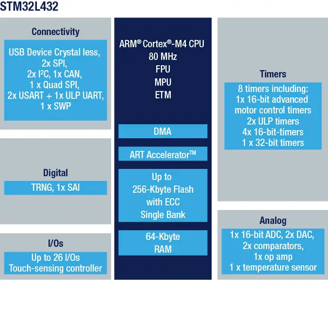
The development boards we’ve selected for this series of tutorials are Nucleo32-L432KC and Blue Pill. Here is the hardware peripherals and ARM-Core highlight diagram for the STM32L432KC microcontroller part.
You can use the STMicroelectronics software tool called “STM32 MCU Finder”. This is basically a parametric searching tool that helps you easily find the convenient microcontroller with the required specs that you select in the GUI tool.
STM32 MCUs We’ll Be Using
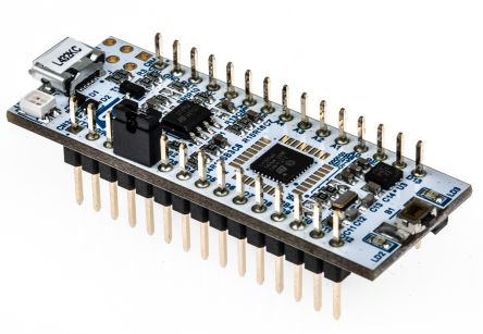
In this series of tutorials, we’ll be using a couple of boards shown down below.
Nucleo32-L432KC
STM32L432KC Datasheet & Documents
Blue Pill STM32F103
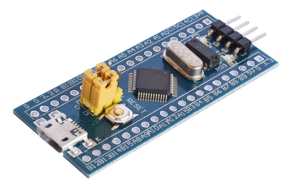
STM32F103C8T6 Datasheet & Documents
ARM Cortex-M4 Processor + FPU
Arm® Cortex®-M4
The Arm® Cortex®-M4 with FPU processor is the latest generation of Arm® processors for embedded systems. It was developed to provide a low-cost platform that meets the needs of MCU implementation, with a reduced pin count and low-power consumption, while delivering outstanding computational performance and an advanced response to interrupts.
The Arm® Cortex®-M4 with FPU 32-bit RISC processor features exceptional code efficiency, delivering the high-performance expected from an Arm® core. The processor supports a set of DSP instructions that allow efficient signal processing and complex algorithm execution.
Its single precision FPU speeds up the software development process and accelerates the target performance. With its embedded Arm® core, the STM32L432KC microcontroller can be used in a wide range of applications. As we’ll see throughout the course.
The other STM32F103C8 microcontroller has a Cortex-M3 core that lacks the FPU and DSP operations which can be a huge miss in certain applications, however, it’s much cheaper target MCU at the end of the day.
Adaptive Real-Time (ART) Accelerator™
The ART Accelerator™ is a memory accelerator that is optimized for STM32 industry-standard Arm® Cortex® M4 processors. It balances the inherent performance advantage of the Arm® Cortex®-M4 over Flash memory technologies, which normally requires the processor to wait for the Flash memory at higher frequencies.
To release the processor near 100 DMIPS performance @ 80MHz, the accelerator implements an instruction prefetch queue and branch cache, which increases program execution speed from the 64-bit Flash memory. Based on the CoreMark benchmark, the performance achieved thanks to the ART accelerator is equivalent to 0 wait state program execution from Flash memory at a CPU frequency up to 80 MHz.
Memory protection unit (MPU)
The memory protection unit (MPU) is used to manage the CPU accesses to memory to prevent one task to accidentally corrupt the memory or resources used by any other active task. This memory area is organized into up to 8 protected areas that can in turn be divided up into 8 subareas.
The MPU is especially helpful for applications where some critical or certified code has to be protected against the misbehavior of other tasks. It is usually managed by an RTOS (realtime operating system). If a program accesses a memory location that is prohibited by the MPU, the RTOS can detect it and take action.
Firewall
The device embeds a Firewall that protects code sensitive and secure data from any access performed by a code executed outside of the protected areas. Each illegal access generates a reset which kills immediately the detected intrusion.
Boot modes
At startup, BOOT0 pin or nSWBOOT0 option bit, and BOOT1 option bit are used to select one of three boot options:
- Boot from user Flash
- Boot from system memory
- Boot from embedded SRAM
BOOT0 value may come from the PH3-BOOT0 pin or from an option bit depending on the value of a user option bit to free the GPIO pad if needed. A Flash empty check mechanism is implemented to force the boot from system flash if the first flash memory location is not programmed and if the boot selection is configured to boot from the main flash.
The boot-loader is located in system memory. It is used to reprogram the Flash memory by using USART, I2C, SPI or USB FS in Device mode through DFU (device firmware upgrade).
System Architecture & Bus Matrix
STM32L432KC (ARM Cortex-M4) Architecture
The system mainly consists of 32-Bit Multilayer AHB Bus Matrix (Highlighted in Yellow) that interconnects the following hardware components:
Five masters:
- Cortex®-M4 with FPU core I-bus
- Cortex®-M4 with FPU core D-bus
- Cortex®-M4 with FPU core S-bus
- DMA1
- DMA2
Seven slaves:
- Internal Flash memory on the ICode bus
- Internal Flash memory on DCode bus
- Internal SRAM1
- Internal SRAM2
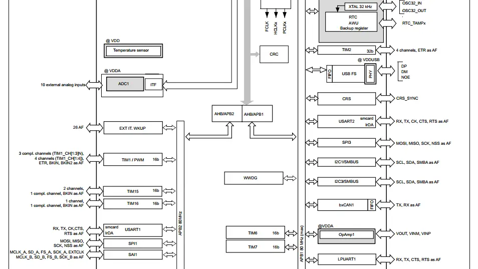
- AHB1 peripherals including AHB to APB bridges and APB peripherals (connected to APB1 and APB2)
- AHB2 peripherals
- The external memory controller (QUAD SPI)
This bus matrix enables multiple masters on the bus to communicate with slaves concurrently. This accelerates the overall performance especially when DMA units are programmed.
The CPU can be doing some calculations and workload while the DMA1 unit is moving the data being received via SPI to SRAM1 memory space. All being done in the same time without CPU intervention or interrupts when every single byte is received.
Multilayer AHB Bus Matrix
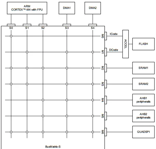
The BusMatrix manages the access arbitration between masters. The arbitration uses a Round Robin algorithm. The BusMatrix is composed of five masters (CPU AHB, system bus, DCode bus, ICode bus, DMA1, and DMA2 bus) and seven slaves (FLASH, SRAM1, SRAM2, AHB1 (including APB1 and APB2), AHB2 and QUAD SPI).
- S0 – I-Bus: This bus connects the instruction bus of the Cortex®-M4 core to the BusMatrix. This bus is used by the core to fetch instructions.
- S1 – D-Bus: This bus connects the data bus of the Cortex®-M4 core to the BusMatrix. This bus is used by the core for literal load and debug access.
- S2 – S-Bus: This bus connects the system bus of the Cortex®-M4 core to the BusMatrix. This bus is used by the core to access data located in a peripheral or SRAM area.
- S3, S4 – DMA-Bus: This bus connects the AHB master interface of the DMA to the BusMatrix.The targets of this bus are the SRAM1 and SRAM2, the AHB1 peripherals including the APB1 and APB2 peripherals, the AHB2 peripherals and the external memories through the QUAD SPI.
AHB/APB Bus Bridges
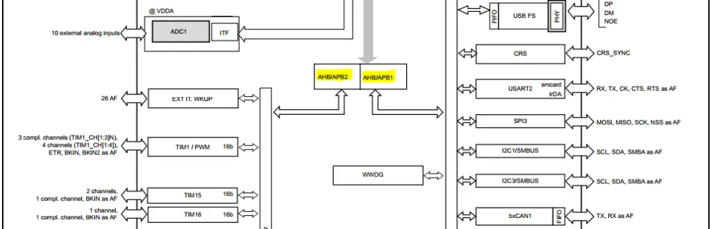
The two AHB/APB bridges provide full synchronous connections between the AHB and the two APB buses, allowing flexible selection of the peripheral frequency. address mapping of the peripherals connected to this bridge.
After each device reset, all peripheral clocks are disabled (except for the SRAM1/2 and Flash memory interface). Before using a peripheral you have to enable its clock in the RCC_AHBxENR and the RCC_APBxENR registers.
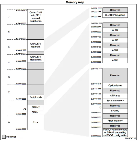
Memory MAP
RCC & Clock Tree
Resect and Clock Control (RCC)
Resect and Clock Control (RCC) Circuitry is our next topic. Let’s just start with the reset circuitry and its functionality. There are three types of reset, defined as system reset, power reset, and backup domain reset.
A Power Reset is generated when one of the following events occurs:
- a Brown-out Reset (BOR).
- when exiting from Standby mode.
- when exiting from Shutdown mode.
A System Reset sets all registers to their reset values unless specified otherwise in the register description. The reset source can be identified by checking the reset flags in the Control/Status register, RCC_CSR. A system reset is generated when one of the following events occurs:
- A low level on the NRST pin (external reset)
- Window watchdog event (WWDG reset)
- Independent watchdog event (IWDG reset)
- A firewall event (FIREWALL reset)
- A software reset (SW reset)
- Low-power mode security reset
- Option byte loader reset
- A Brown-out reset
The Software Reset: The SYSRESETREQ bit in Cortex®-M4 Application Interrupt and Reset Control Register must be set to force a software reset on the device.
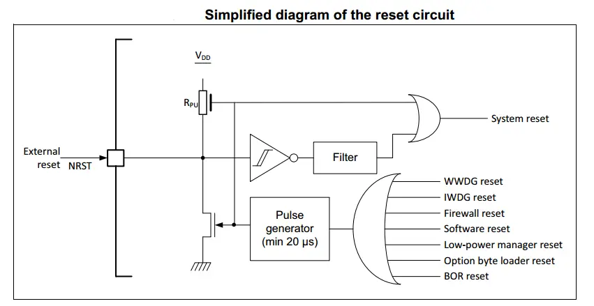
The Backup Domain Reset has two specific reset signals. A backup domain reset is generated when one of the following events occurs:
- Software reset, triggered by setting the BDRST bit in the Backup domain control register (RCC_BDCR).
- VDD or VBAT power on, if both supplies have previously been powered off. A backup domain reset only affects the LSE oscillator, the RTC, the Backup registers, and the RCC Backup domain control register.
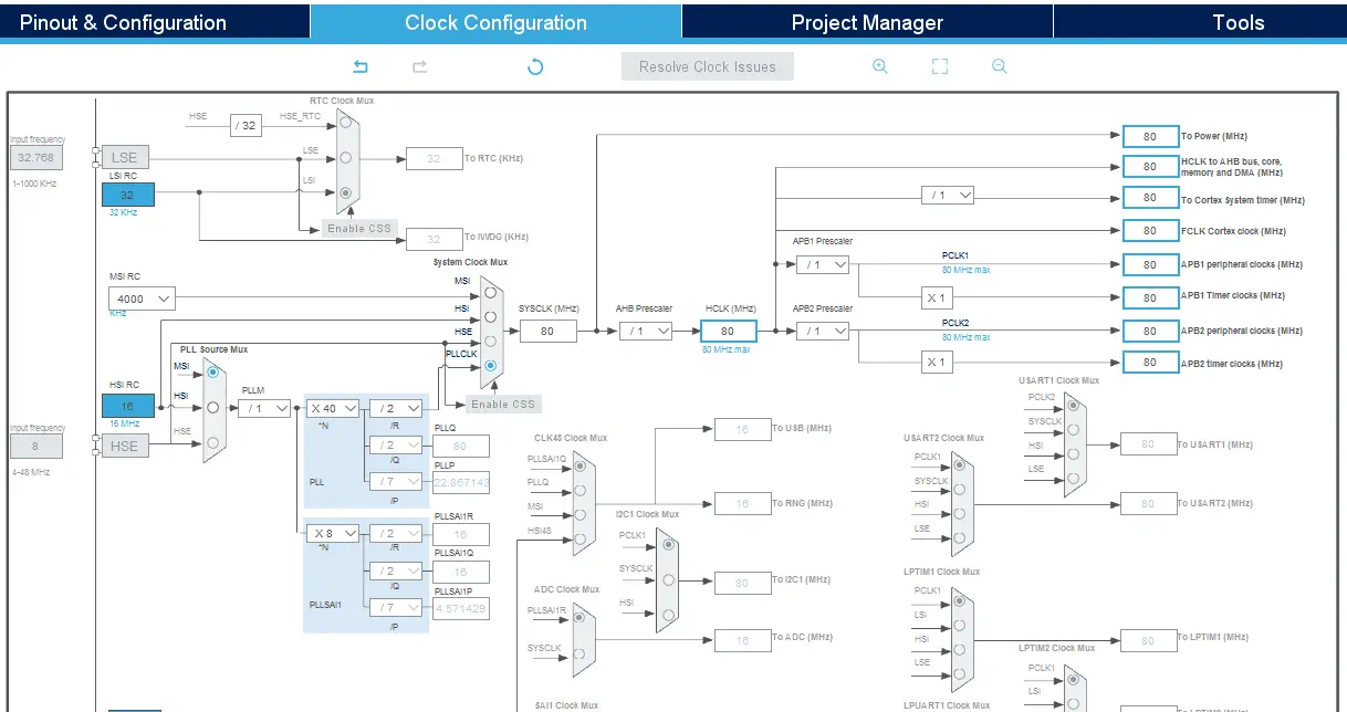
Clock Tree
Four different clock sources can be used to drive the system clock (SYSCLK):
- HSI16 (high speed internal)16 MHz RC oscillator clock
- MSI (multispeed internal) RC oscillator clock
- HSE oscillator clock, from 4 to 48 MHz
- PLL clock
The MSI is used as system clock source after startup from Reset, configured at 4 MHz.
The devices have the following additional clock sources:
- 32 kHz low-speed internal RC (LSI RC) which drives the independent watchdog and optionally the RTC used for Auto-wakeup from Stop and Standby modes.
- 32.768 kHz low-speed external crystal (LSE crystal) which optionally drives the realtime clock (RTCCLK).
- RC 48 MHz internal clock sources (HSI48) to potentially drive the USB FS, the SDMMC and the RNG.
Each clock source can be switched on or off independently when it is not used, to optimize power consumption.
We’ll be using CubeMX in the step of configuring the clock tree. Where we can set the desired SYSCLK speed (up to 80MHz for L432KC or up to 72MHz for F103C8). And we can also set the clock speed for the different peripherals, buses, and the USB hardware as well.
And that’s it for this tutorial. In the next one, we’ll get a closer look at the LL + HAL libraries that we’ll be using later on by configuring the CubeMX software tool. Afterward, we shall start getting into the hardware peripherals and starts doing some practical LAB examples.
| Previous Tutorial | Tutorial 1 | Next Tutorial | |||||
I am reading stm32 tutorial right after reading the pic tutorials. I must say that your pic tutorials were great and you tried to explain everything in a very simple language. But stm32 tutorial seems to be written in hurry and not much explanation given of the terms used. It will be helpful if you can explain first the difference between stm32 and pic, difference in the tools used. For example,why stm32cubeMx is used and what is LL and HAL driver?how different is developing firmware for pic from developing firmware for stm32?
Thanks
Hi Anubhav! First, I’d like to really thank you for taking the time to give me your honest feedback about this work. And also for following the previous series of tutorials (using 8-Bit Microchip PIC devices). By the way, I’m still not over with it and should be able to continue some more interfacing tutorials in the future as many readers have suggested (things like GSM, GPS, TFT, RTC, and so on).
The key difference between the way I’ve planned this new course to be and the previous one is:
Now I’m assuming the reader has a solid introduction for how the low-level hardware works, and we’ve been playing around with the bits, flags, and byte at the low layers of software. This knowledge is assumed to be acquired.
And therefore, I’ve given an introduction to the new hardware architecture of the ARM-Based STM32 devices. And also introduced the software architecture we’ll be sticking to. It shows all the software layers including the LL & HAL from STMicroelectronics and the application layers (which we’ll be developing throughout the course).
To conclude this and answer your question, the key difference is that we’ve shifted the focus of development effort from the low-level hardware drivers to the application layer & ECU abstraction layer. I was and I’m still believing that this will add too much value for the readers and help engineers structure the system in a better way and write a portable code that can be easily ported across the STM32 portfolio of microcontrollers.
One last thing, I’d really appreciate if you check the GitHub repo for the course and have a look how the application layer drivers are easily configurable and the programmer doesn’t write an ultrasonic driver that is hard-programmer for a specific timer and takes a tremendous effort to port a complete application from a target to another.
It was a little bit long comment XD! But I hope this makes things a little bit clearer and reveal my intentions and vision about this course.
Kind regards,
Khaled M.
Thanks,
Sorry my English is not good, but I am reading, reading not studying this course, which to my understanding is fantastic and very objective, which is to teach about STM32.
And I want to congratulate you for this beautiful attitude in sharing your knowledge.
Thank you very much, and you can be sure that I will follow and share.
Fernando
Thanks for your great effort.
If you can make explanation video, those are very helpful.
Thanks for your help
This pages are the most completed that I’ve found to learn step by step STM32 .. more than 40 tutorials, with a lot of hardware gadgets …
Congratulations and keep your good job ..
Regards,
Luís
Thanks so much, Luís for your kind words!
I’m really glad that it did help you.
All the best,
Can I use the STM32 black pill instead?
Sure, you can! Any STM32 Dev board will work just as fine in almost all tutorials. If you’ve encountered any issues using a different board in any tutorial, just drop me a comment there, I’ll be glad to help.
Good luck ^^