| Previous Tutorial | Tutorial 27 | Next Tutorial | |||||
| STM32 DAC Tutorial With Examples To Generate Analog Signals | |||||||
| STM32 Course Home Page ???? | |||||||
In this tutorial, we’ll discuss the STM32 DAC (Digital-To-Analog Converter) module. Starting with an introduction for the DAC as a digital circuit and then shifting the attention to the STM32 DAC hardware and its features. We’ll get into the functional description for the DAC in STM32 microcontrollers, how it works, and how to configure it and make the best use of it. And let’s get right into it!
[toc]
Required Components For LABs
All the example code/LABs/projects in the course are going to be done using those boards below.
- Nucleo32-L432KC (ARM Cortex-M4 @ 80MHz) or (eBay)
- Blue Pill STM32-F103 (ARM Cortex-M3 @ 72MHz) or (eBay)
- ST-Link v2 Debugger or (eBay)
| QTY | Component Name | ???? Amazon.com | ???? eBay.com |
| 2 | BreadBoard | Amazon | eBay |
| 1 | LEDs Kit | Amazon Amazon | eBay |
| 1 | Resistors Kit | Amazon Amazon | eBay |
| 1 | Capacitors Kit | Amazon Amazon | eBay & eBay |
| 2 | Jumper Wires Pack | Amazon Amazon | eBay & eBay |
| 1 | 9v Battery or DC Power Supply | Amazon Amazon Amazon | eBay |
| 1 | Micro USB Cable | Amazon | eBay |
| 1 | Push Buttons | Amazon Amazon | eBay |
★ Check The Full Course Complete Kit List
Some Extremely Useful Test Equipment For Troubleshooting:
- My Digital Storage Oscilloscope (DSO): Siglent SDS1104 (on Amazon.com) (on eBay)
- FeelTech DDS Function Generator: KKMoon FY6900 (on Amazon.com) (on eBay)
- Logic Analyzer (on Amazon.com) (on eBay)
Affiliate Disclosure: When you click on links in this section and make a purchase, this can result in this site earning a commission. Affiliate programs and affiliations include, but are not limited to, the eBay Partner Network (EPN) and Amazon.com.
Digital-To-Analog Converters (DAC) Preface
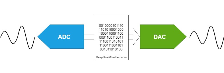
A DAC (Digital-To-Analog) converter is an electronic circuit that takes in a digital number or value as an input and converts it into an analog voltage, the voltage level that corresponds to the binary number in the DAC output register. The DAC output voltage changes whenever you change the DAC output register value, and this sampling process can be triggered in multiple ways as we’ll see hereafter.
The DAC does the inverse operation that of an ADC, while an ADC (A/D) converts analog voltage to digital data the DAC (D/A) converts digital numbers to the analog voltage on the output pin.
Not all microcontrollers come with on-chip DAC peripheral that’s why we usually use external DAC ICs or perform some techniques like PWM-To-DAC conversion as we shall see in the upcoming tutorials. But the point here is that the Blue Pill (STM32F103C8) doesn’t have an internal DAC module while the Nucleo32-L432KC does have two. Therefore, in this tutorial, we’ll be working with the Nucleo32-L432KC DAC module and test it in a couple of LABs. And in the upcoming tutorials, we’ll see how to achieve DAC operation on the blue pill development board even without having the hardware peripheral.
For those who would like to have a solid introduction in the DAC module, how it works at the low level, different types of DACs, errors, equations, and all other details. The DAC Tutorial down below is a complete introductory guide for this topic and highly recommended.
STM32 DAC Brief
In STM32L432KC, the DAC module is a 12-bit, voltage-output digital-to-analog converter. The DAC can be configured in 8- or 12-bit mode and may be used in conjunction with the DMA controller. In 12-bit mode, the data could be left- or right-aligned. The DAC features up to two output channels, each with its own converter. In dual DAC channel mode, conversions could be done independently or simultaneously when both channels are grouped together for synchronous update operations.
The DAC_OUTx pin can be used as general-purpose input/output (GPIO) when the DAC output is disconnected from the output pad and connected to on-chip peripherals. The DAC output buffer can be optionally enabled to allow a high drive output current. An individual calibration can be applied to each DAC output channel. The DAC output channels support a low power mode, the Sample and Hold mode.
DAC Features
- One DAC interface, maximum of two output channels
- Left or right data alignment in 12-bit mode
- Synchronized update capability
- Noise-wave and Triangular-wave generation
- Dual DAC channel for independent or simultaneous conversions
- DMA capability for each channel including DMA underrun error detection
- External triggers for conversion
- DAC output channel buffered/unbuffered modes
- Buffer offset calibration
- Each DAC output can be disconnected from the DAC_OUTx output pin
- DAC output connection to on-chip peripherals
- Sample and Hold mode for low power operation in Stop mode
- Input voltage reference, VREF+
STM32 DAC Functional Description
STM32 DAC Block Diagram
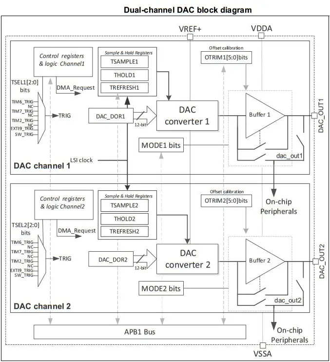
The DAC includes up to two separate output channels. Each output channel can be connected to on-chip peripherals such as comparator, operational amplifier, and ADC (if available). In this case, the DAC output channel can be disconnected from the DAC_OUTx output pin and the corresponding GPIO can be used for another purpose. The DAC output can be buffered or not.
Each DAC channel can be powered on by setting its corresponding ENx bit in the DAC_CR register. The DAC channel is then enabled after a tWAKEUP startup time.
STM32 DAC Data Format
Depending on the selected configuration mode, the data have to be written into the specified register as described below:
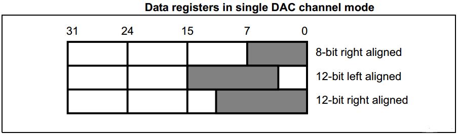
Single DAC channel
There are three possibilities:
- 8-bit right alignment: the software has to load data into the DAC_DHR8Rx[7:0] bits (stored into the DHRx[11:4] bits)
- 12-bit left alignment: the software has to load data into the DAC_DHR12Lx [15:4] bits (stored into the DHRx[11:0] bits)
- 12-bit right alignment: the software has to load data into the DAC_DHR12Rx [11:0] bits (stored into the DHRx[11:0] bits)
Depending on the loaded DAC_DHRyyyx register, the data written by the user is shifted and stored into the corresponding DHRx (data holding registerx, which are internal non-memory mapped registers). The DHRx register is then loaded into the DORx register either automatically, by software trigger, or by an external event trigger.
 STM32 DAC Conversion
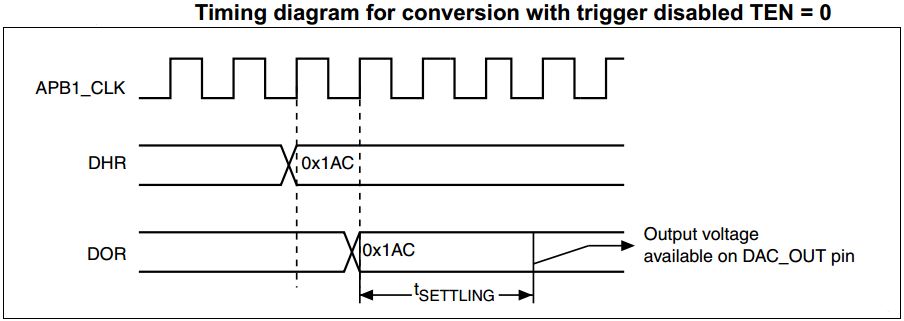
The DAC_DORx cannot be written directly and any data transfer to the DAC channelx must be performed by loading the DAC_DHRx register (write operation to DAC_DHR8Rx, DAC_DHR12Lx, DAC_DHR12Rx, DAC_DHR8RD, DAC_DHR12RD or DAC_DHR12LD).
Data stored in the DAC_DHRx register are automatically transferred to the DAC_DORx register after one APB1 clock cycle if no hardware trigger is selected (TENx bit in DAC_CR register is reset). However, when a hardware trigger is selected (TENx bit in DAC_CR register is set) and a trigger occurs, the transfer is performed three APB1 clock cycles after the trigger signal.
When DAC_DORx is loaded with the DAC_DHRx contents, the analog output voltage becomes available after a time tSETTLING that depends on the power supply voltage and the analog output load.
STM32 DAC Output Voltage Equation (Formula)
Digital inputs are converted to output voltages on a linear conversion between 0 and VREF+. The analog output voltages on each DAC channel pin are determined by the following equation:
DACoutput = (VREF+) x (DOR/4096)
DAC Noise Generation
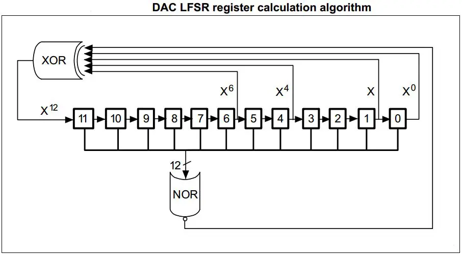
In order to generate a variable-amplitude pseudo-noise, an LFSR (linear feedback shift register) is available. DAC noise generation is selected by setting WAVEx[1:0] to 01”. The preloaded value in LFSR is 0xAAA. This register is updated three APB1 clock cycles after each trigger event, following a specific calculation algorithm.
STM32 DAC Channel Modes of Operation
Each DAC channel can be configured in Normal mode or Sample and Hold mode. The output buffer can be enabled to allow a high drive capability. Before enabling the output buffer, the voltage offset needs to be calibrated. This calibration is performed at the factory (loaded after reset) and can be adjusted by software during application operation.
Normal Mode
In Normal mode, there are four combinations, by changing the buffer state, and by changing the DAC_OUTx pin interconnections.
To enable the output buffer, the MODEx[2:0] bits in DAC_MCR register should be:
- 000: DAC is connected to the external pin
- 001: DAC is connected to the external pin and to on-chip peripherals
To disable the output buffer, the MODEx[2:0] bits in DAC_MCR register should be:
- 010: DAC is connected to the external pin
- 011: DAC is connected to on-chip peripherals
Sample And Hold Mode
In sample and Hold mode, the DAC core converts data on a triggered conversion, then, holds the converted voltage on a capacitor. When not converting, the DAC cores and buffer are completely turned off between samples and the DAC output is tri-stated, therefore reducing the overall power consumption. A new stabilization period, which value depends on the buffer state, is required before each new conversion.
In this mode, the DAC core and all corresponding logic and registers are driven by the low-speed clock (LSI) in addition to the APB1 clock, allowing to use the DAC channels in deep low power modes such as Stop mode.
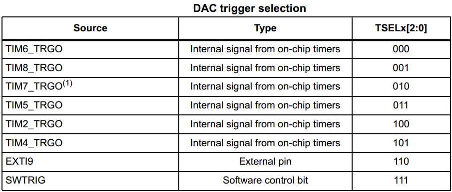
DAC Conversion On External Triggers
If the TENx control bit is set, conversion can then be triggered by an external event (timer counter, external interrupt line). The TSELx[2:0] control bits determine which out of 8 possible events will trigger conversion.
Each time a DAC interface detects a rising edge on the selected trigger source, the last data stored into the DAC_DHRx register are transferred into the DAC_DORx register. The DAC_DORx register is updated three APB1 cycles after the trigger occurs.
If the software trigger is selected, the conversion starts once the SWTRIG bit is set. SWTRIG is reset by hardware once the DAC_DORx register has been loaded with the DAC_DHRx register contents.
STM32 DAC Calibration
The transfer function for an N-bit digital-to-analog converter (DAC) is:
VOUT = ((D/2N-1) x G x Vref) + Vos
Where VOUT is the analog output, D is the digital input, G is the gain, Vref is the nominal fullscale voltage, and Vos is the offset voltage. For an ideal DAC channel, G = 1 and Vos = 0.
Due to output buffer characteristics, the voltage offset may differ from part-to-part and introduce an absolute offset error on the analog output. To compensate the Vos, a calibration is required by a trimming technique. The calibration is only valid when the DAC channelx is operating with buffer enabled (MODEx[2:0] = 000b or 001b or 100b or 101b). if applied in other modes when the buffer is off, it has no effect. During the calibration:
- The buffer output will be disconnected from the pin internal/external connections and put in tristate mode (HiZ),
- The buffer will act as a comparator, to sense the middle-code value 0x800 and compare it to VREF+/2 signal through an internal bridge, then toggle its output signal to 0 or 1 depending on the comparison result (CAL_FLAGx bit)
Two calibration techniques are provided:
- Factory trimming: (always enabled) The DAC buffer offset is factory trimmed. The default value of OTRIMx[4:0] bits in the DAC_CCR register is the factory trimming value and it is loaded once DAC digital interface is reset.
- User trimming: The user trimming can be done when the operating conditions differ from nominal factory trimming conditions and in particular when VDD/VDDA voltage, temperature, VREF+ values change and can be done at any point during application by software.
The STM32 HAL does provide a function within the DAC APIs dedicated to starting the calibration process and as said before it’s a recommended step after initializing the DAC hardware at the system power-up in case your operating conditions are different from the nominal factory settings. Otherwise, you can use the factory calibration settings.
STM32 DAC Resolution, Reference, Formulas
STM32 DAC Resolution
The STM32 DAC has a resolution of 12-Bit that can be configured to be 8-bit as well. Depending on your application you can choose between the two options and obviously the 12-Bit resolution is great for audio applications.
DAC Reference Voltage
The DAC reference voltage can be configured to be from an external pin or provided internally using the internal VREFBUF module. The reference voltage you’ll choose for the DAC operation will define the maximum allowable voltage swing as well as the output voltage resolution.
STM32 DAC Formulas
DAC Output Voltage
VOUT = DOR x (Reference Voltage / 4096)
Where Reference Voltage = (VREF+) – (VREF-)
DAC & DMA
Each DAC channel has a DMA capability. Two DMA channels are used to service DAC channel DMA requests. When an external trigger (but not a software trigger) occurs while the DMAENx bit is set, the value of the DAC_DHRx register is transferred into the DAC_DORx register when the transfer is complete, and a DMA request is generated.
In dual-mode, if both DMAENx bits are set, two DMA requests are generated. If only one DMA request is needed, only the corresponding DMAENx bit should be set. In this way, the application can manage both DAC channels in dual mode by using one DMA request and a unique DMA channel.
DAC DMA Underrun
The DAC DMA request is not queued so that if a second external trigger arrives before the acknowledgment for the first external trigger is received (first request), then no new request is issued and the DMA channelx underrun flag DMAUDRx in the DAC_SR register is set, reporting the error condition. The DAC channelx continues to convert old data.
The software should clear the DMAUDRx flag by writing 1, clear the DMAEN bit of the used DMA stream, and re-initialize both DMA and DAC channelx to restart the transfer correctly. The software should modify the DAC trigger conversion frequency or lighten the DMA workload to avoid a new DMA underrun. Finally, the DAC conversion could be resumed by enabling both DMA data transfer and conversion trigger.
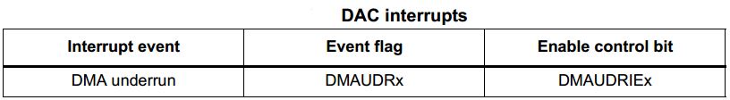
STM32 DAC Interrupts
Only one interrupt signal can be fired on a DAC DMA Underrun condition.
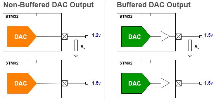
STM32 DAC Buffered-Output Vs Non-Buffered
Every electronic circuit has an input impedance that represents a load resistance for whatever stage that precedes this circuit. For a DAC, the output voltage will be loaded if you connect the DAC_OUT pin to whatever circuit maybe to amplify it or filter it or whatever. The existence of output load resistance will draw a little bit of current that results in a voltage shift (drop) on the DAC output.
Therefore, we always need to buffer the DAC output if we’re going to hook it up to another electronic circuit. An output buffer is an op-amp that works in a voltage follower configuration which will source current to the load resistance at the output and do whatever it takes to make sure that the DAC_OUT voltage is what it should be (identical to its input). Down below is an example comparison between a buffered DAC and non-buffered DAC output. Both of which are being tested in no-load and loaded configurations. And both of which are programmed to produce 1.5v on the DAC_OUT pin.
STM32 DAC Speed (Sampling Rate)
Output Buffer Effect & Output Impedance, Capacitance
When the output buffer is enabled on the DAC output, the speed is specified by the output buffer performance. This number is indicated in the Tsettling or Update rate in the product datasheet.
When the output buffer is disabled, the output signal speed simply follows the RC constant, which is determined by the DAC output impedance RDAC (= 2 x Ra) and the capacitive load on the DAC_OUT pad.
As an example, the STM32F407 defines the impedance output with the buffer off at a maximum value of 15 kΩ. If a 10 pF capacitive load (including the parasitic capacitance of the STM32F407 device on DAC_OUT pad) is considered, to get ±1 LSB of the final value (from lowest code to highest code) we have:
1 – (1/2N) = 1 – e(T/RC)
Solving for T gives T = CR x N x ln(2) = 0.693 x RC x N = 1.8 µs, hence, in this configuration, the conversion time cannot be smaller than 1.8 µs (equivalent to a frequency of 555 kHz). This analysis does not include any effect of the switching speed of the DAC itself and its transient. When using high speed, these factors cannot be ignored, they degrade the performance.
Digital Data Update Rate
The STM32 DAC output data need to be written to the DAC holding register (DHR), then the data is moved to the DAC output register (DOR) for the conversion. Generally, the data are saved in a RAM, and the CPU is in charge of transferring the data from RAM to DAC.
When using the DMA, the overall performance of the system is increased by freeing up the core. This is because data is moved from memory to DAC by DMA, without the need for any actions by the CPU. This keeps CPU resources free for other operations. The trigger of the DAC conversion can be done by the software, external triggers, or by the timers. For the high-speed conversion cases, it is recommended to use the timer trigger in combination with the data transfer done by the DMA.
The transfer speed from memory to the DAC is limited by several factors, among them:
- The clock cycle of the APB or of the AHB (DAC clock)
- The DMA transfer cycle from memory to the DAC (includes the AHB to APB bridge)
- The trigger mechanism itself
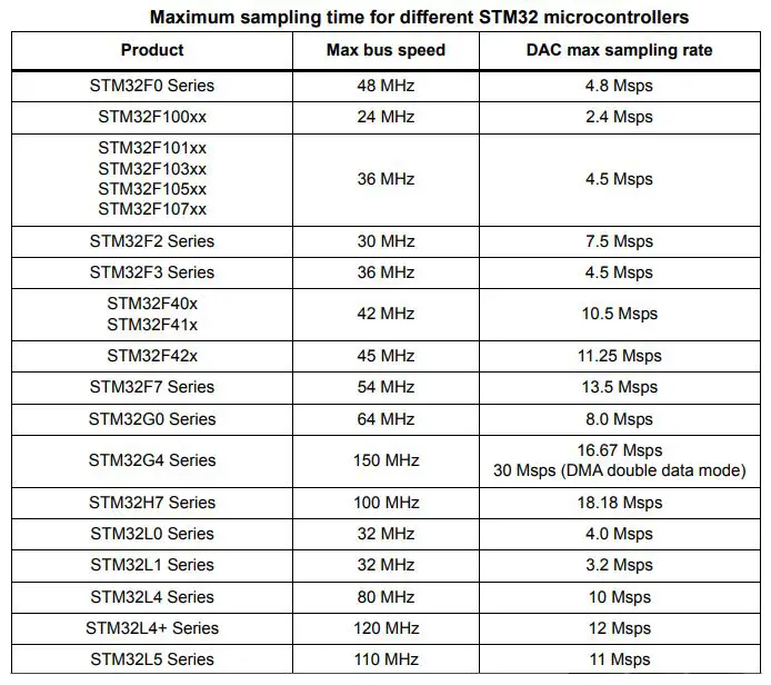
Here is a table for the maximum sampling rates that can be achieved on various STM32 devices’ DAC peripherals.
DAC Example Applications
In the next few tutorials, we’ll be practicing the DAC peripheral and do some practical LABs in order to learn how to configure and program the DAC to do certain tasks in different ways. The DAC example applications will include the following:
- Analog Voltage Output
- Analog Waveform Generation (Sine, Sawtooth, Triangular)
- Audio Production
STM32 DAC Example – LAB22
| LAB Number | 22 |
| LAB Title | STM32 DAC Basic LAB |
- Set up a new project as usual with system clock @ 80MHz
- Set up the DAC1 peripheral to work in normal mode with output buffer enabled
- Output the following voltage pattern 0v, 1v, 2v, 3v, every 50ms and repeat
The output voltage on the DAC_OUT pin is expected to be like shown in this diagram below.
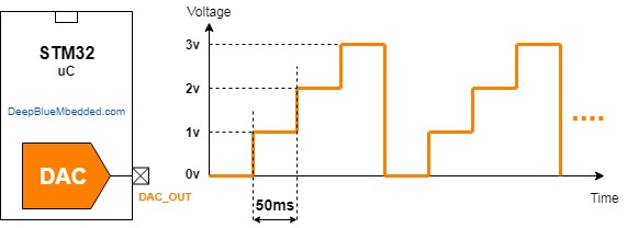
In this LAB project, we’ll initialize the DAC module. And write to it value each 50msec time interval. The DAC output voltage is required to go in the following pattern (0v, 1v, 2v, 3v). The corresponding digital values are as follows:
For 1v output, the DOR is calculated from
Vout = DOR x (VREF / 4096)
1v = DOR x (3.3 / 4096)
=> DOR = 1241
And so on for the other voltages.
And now, let’s build this system step-by-step
Step1: Open CubeMX & Create New Project
Step2: Choose The Target MCU & Double-Click Its Name
STM32L432KC
Step3: Go To The Clock Configuration
Step4: Set The System Clock To Be 80MHz
Step5: Enable The DAC1 Output In Normal Mode & Buffer Enable
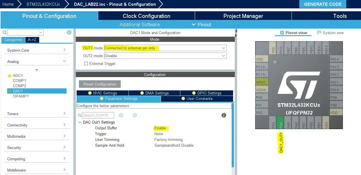
Step6: Generate The Initialization Code & Open The Project In Your IDE
Here is The Application Code For This LAB (main.c)
|
1 2 3 4 5 6 7 8 9 10 11 12 13 14 15 16 17 18 19 20 21 22 23 24 25 26 27 28 |
#include "main.h" DAC_HandleTypeDef hdac1; void SystemClock_Config(void); static void MX_GPIO_Init(void); static void MX_DAC1_Init(void); int main(void) { uint32_t DAC_OUT[4] = {0, 1241, 2482, 3723}; uint8_t i = 0; HAL_Init(); SystemClock_Config(); MX_GPIO_Init(); MX_DAC1_Init(); while (1) { DAC1->DHR12R1 = DAC_OUT[i++]; if(i == 4) { i = 0; } HAL_Delay(50); } } |
Download The STM32 DAC Project LAB22
The Result For LAB Testing On My DSO
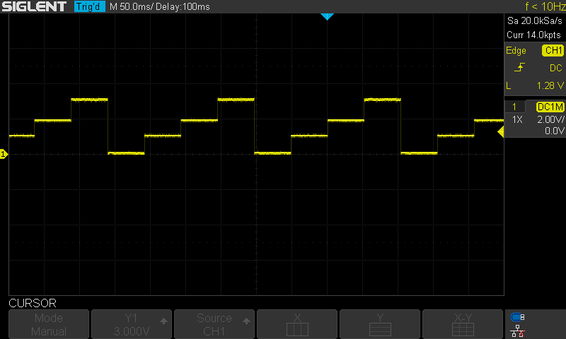
Exactly like what we’ve expected it to be!
In the next tutorial, we’ll see how to generate analog waveforms like sine, sawtooth, etc. Using the DAC module and in different ways.
Did you find this helpful? If yes, please consider supporting this work and sharing these tutorials!
Stay tuned for the upcoming tutorials and don’t forget to SHARE these tutorials. And consider SUPPORTING this work to keep publishing free content just like this!
| Previous Tutorial | Tutorial 27 | Next Tutorial | |||||
I couldn’t get this to work until I added this line before the WHILE loop:
HAL_DAC_Start(&hdac1, DAC1_CHANNEL_1);
Indeed! Thanks
yes, you need to start it…same as timers
I tried to check the stm32f1xx_hal_msp.c file. There is a function that initializes the GPIO pin for the DAC to operate in the ANALOG mode. And it does also enable the DAC clock. All this happens when you call HAL_Init();
Now, I’ll need to check what the DAC_Start function does to make sure that it’s something else that is missing other than the clock enable.
Hi Khaled – thanks for the great tutorial series. Really appreciate all the effort you’ve put into this. It’s really helping me to get to grips with the STM32, quickly!
Like Martin, I couldn’t get the DAC tutorial to work, because I hadn’t started the DAC. I had a little dig around in the *_hal_dac.c file, and ended up with the following (working) code to write the DAC on each iteration of the while(1) loop:
HAL_DAC_SetValue(&hdac, DAC_CHANNEL_1, DAC_ALIGN_12B_R, dacValues[dacIndex]);
HAL_DAC_Start(&hdac, DAC_CHANNEL_1);
Obviously the ‘HAL_DAC_SetValue()’ method is just a wrapper around the write to the DAC_DHR12R1 register. You’ve used the HAL wrappers for register access in all your other tutorials so far. Was there any reason why you chose not to use it this time?
Thanks again.
Mk