| Previous Tutorial | Tutorial 21 | Next Tutorial | |||||
| SPI Tutorial | Serial Peripheral Interface | |||||||
| Intermediate Level ★★☆☆☆ | |||||||
In this tutorial, we’ll be discussing the SPI (serial peripheral interface) bus. How it works and how to establish serial communication between 2 PIC microcontrollers via SPI. This is going to be an extensively detailed guide for the ins and outs of the SPI communication in general, and programming PIC MCUs to be SPI master/slave in particular on MPLAB IDE and XC8 Compiler. So, it’s essentially a long-read and hopefully helpful. And let’s get started!
[toc]
Required Components
| Qty. | Component Name | Buy On Amazon.com |
| 2 | PIC16F877A | Add |
| 2 | BreadBoard | Add |
| 8 | LED | Add Add |
| 1 | Resistors Kit | Add Add |
| 1 | Capacitors Kit | Add Add |
| 1 | Jumper Wires Pack | Add Add |
| 1 | LM7805 Voltage Regulator (5v) | Add |
| 1 | Crystal Oscillator | Add |
| 1 | PICkit2 or 3 Programmer | Add |
| 2 | 9v Battery or DC Power Supply | Add Add Add |
Serial Communication Introduction (Review)
[ Disclaimer: This section has been discussed earlier in Tutorial-18 For UART. If you’ve already read it, just skip to the next one. ]
In Embedded Systems, Telecommunication, and Data Transmission applications, Serial Communication is known to be the process of sending data one bit at a time (bit-by-bit) sequentially, over the serial bus. It takes a complete clock cycle in order to transfer each bit from an end to the other. Conversely, parallel communication is known to be the process of sending several bits, even bytes, as a whole only in a single clock cycle. However, even if you transfer fewer data per cycle with a serial transmission, you can do it at much higher frequencies which results in higher net transfer rates than of the parallel communication.
The Fundamental Concepts
There do exist many serial communication protocols, each of which is working in a different way. However, it turns out to be some similarity that they do share in common. Frankly speaking, serial communication protocols have Shift Registers somehow/somewhere in their hardware implementation as the working-horse (core). Shift registers are used to shift out the data to be transmitted bit-by-bit each clock cycle. So, let’s dig deeper into a shift register in order to build up a complete understanding of what is actually happening at the Register(low)-Level.
Shift registers are basically some D-Flip-Flops serially connected while sharing the same clock line. Here is a graphical animation that demonstrates how does a shift register work internally.
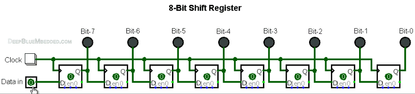
As you might have noticed, the data input (0’s and 1’s) is being shifted from the input pin to the output end at bit-0. It takes only 1-clock to transfer a single bit, which means it takes 8-clocks for a single byte transfer. For the same of simplicity, we’ll represent the shift register as a single block instead of a series of D-Flip-Flops as shown above.
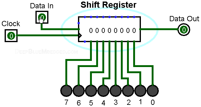
Here is an animation for an 8-Bit shift register with a serial input & serial output data lines.
Well, now you should know how shift registers are actually working. Frankly speaking, serial communication is as simple as connecting a couple of shift registers together! Connecting the data output of a shift register to be the data input of the other shift register enables us of sending digital data serially from an end to another!
In the following animation, I’m connecting a couple of 4-Bit shift registers. One at the transmitter device and the other at the receiver device. The serial bus consists of a couple of wires (data, and clock). Each clock, a bit is sent from the transmitter TX pin and received by the receiver’s RX pin.
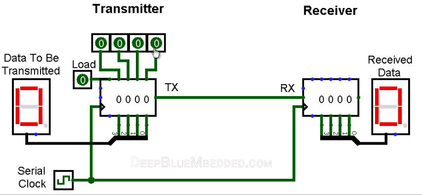
As you might have noticed, it takes 4-clocks to send the 4-Bit data from the transmitter to the receiver. This is simply the short answer to the “How Serial Communication Works?”. However, it’s not everything you should know about serial communication or at least to the level of being able to implement a simple serial data transfer process.
In fact, there are some other options and configurations for each serial communication protocols. Which includes, various data transmission rates, error detection, and correction mechanisms, and much more that adds to the overall complexity associated with each protocol. We’ll be working with the UART protocol in this tutorial, which has a decent steep learning curve.
Serial VS Parallel Communication
As we’ve stated earlier, serial communication is the process of sending data each bit at a time (bit-by-bit). And conversely, parallel communication is the process of sending multiple bits, even bytes, as a whole in a single clock cycle.
A very basic implementation, that you can create on your own, for the parallel data transfer is shown down below. As I’m connecting a couple of 4-Bit registers, via the 5-wire parallel bus (4-data pins + 1-clock). Here is an animation that shows you how parallel data transfer is done.
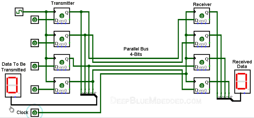
As you might have noticed, it takes only 1-clock to transfer the data from a transmitter device to the receiver! Frankly speaking, we can theoretically transfer any number of bits (or bytes) using parallel communication protocols in a single clock cycle at a time.
Here is a brief comparison between serial communication and parallel communication protocols.
| Feature | Serial Communication | Parallel Communication |
| Relative Speed | Faster | Slower |
| Distance Range | Much Farther | Shorter |
| Transfer Method | One bit is transmitted at a time | Bytes are transmitted in parallel, One byte or more at a time |
| Applications | Computer small peripherals, modules interfacing, and sensors measuring & sending simple data frames | Short distance High-Speed communication such as Computer printers, etc |
| Wires Inside | Few wires, all data bits pass only through the same data line | Multiple, more wires, each bit has a dedicated wire. So as to be transmitted all at once |
| Cables Pictures | 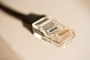 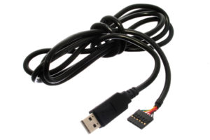  |
   |
Applications Of Serial Communication Protocols
There are countless situations in which we do use one or more of the serial communication protocols. Here, I’ll try to categorize the main purposes for which we use serial communication instead of listing down all possible applications that may be serving the same purposes. Hence, any application will, hopefully, possibly fall under the umbrella of the following purposes.
- External devices/modules communications
- Downloading / Updating The Firmware
- Console io
- Data Transmission
- Debugging interface
Serial communication protocols are of fundamental importance for each embedded systems application. And as embedded systems engineers, we must have a very good experience with almost all of the commonly used serial communication protocols. And in the next sub-section, we’ll see a brief collection of the commonly available serial communication protocols in the embedded market.
Examples Of Serial Communication Protocols
There are many serial communication protocols that are existent and being used in various domains and sub-domains of embedded systems. Some of which are more likely to be used in the automotive industry such as LIN & CAN, some of which is more likely to be used for external memory interfacing as I2C, high-speed computer interfacing as USB, and for audio applications such as I2S. Here is a list of the most common serial communication protocols in the industry.
| USB | CAN | I2C |
| I2S | LIN | SPI |
| Ethernet | 1-Wire | UART/USART |
| And many others… | ||
We’ll be focusing only on the SPI serial peripheral interface for the rest of this tutorial. Just to understand the fundamentals & mechanics of SPI communication. Only then, we’ll be able to develop the necessary firmware in order to transmit data from an embedded MCU to another as we’ll be doing the lab at the end of this tutorial. So, let’s get started with SPI.
SPI | And How It Works?
What’s SPI? And How it Works?
SPI is an acronym for (Serial Peripheral Interface) pronounced as “S-P-I” or “Spy”. Which is an interface bus typically used for serial communication between microcomputer systems and other devices, memories, and sensors. Usually used to interface Flash Memories, ADC, DAC, RTC, LCD, SDcards, and much more.
The SPI was originally developed by Motorola back in the 80s to provide full-duplex serial communication to be used in embedded systems applications.
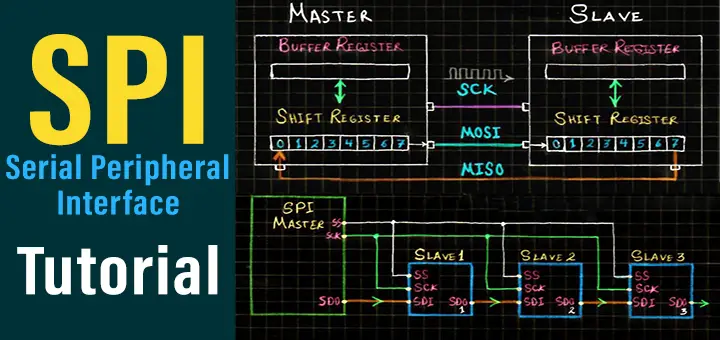
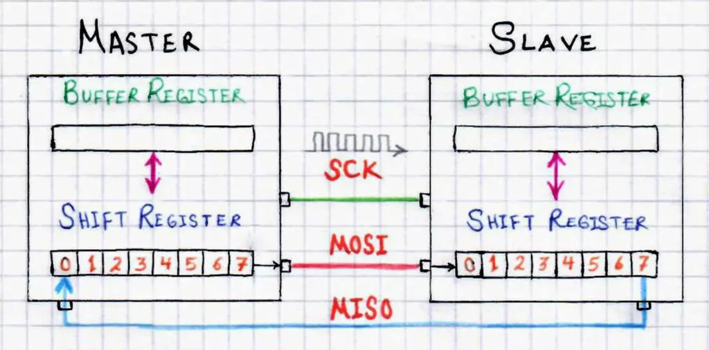
In typical SPI communication, there should be at least 2 devices attached to the SPI bus. One of them should be the master and the other will essentially be a slave. The master initiates communication by generating a serial clock signal to shift a data frame out, at the same time serial data is being shifted-in to the master. This process is the same whether it’s a read or write operation.
Pin Conventions & Connections
The SPI bus includes 4 logic lines defined as follows:
MISO -> Master input slave output (Dout From Slave).
MOSI -> Master output slave input (Dout From Master).
SCLK -> Serial Clock, generated by the master and goes to the slave.
SS -> Slave Select. Generated by the master to control which slave to talk to. It’s usually an active-low signal.
Other naming conventions are followed by different manufacturers across the globe. But in the end, they are referring to the same things. Here are some of the commonly used terms to express the above 4 logic lines (SPI Bus).
MISO (master in slave out) => can also be SIMO, DOUT, DO, SDO, or SO (At The Master End).
MOSI (master out slave in) => can also be SOMI, DIN, DI, SDI, or SI (At The Master End).
SS (slave select) => can also be CE, CS, or SSEL.
SCLK (serial clock) => can also be SCK.
The convention we’re going to follow in this tutorial and upcoming topics related to SPI will be the following one
[ SDI, SDO, SCK, SS]
The typical SPI connection between a single master and a single slave is indicated in the diagram below.
Modes of Operation
Devices on the SPI bus can operate in either mode of the following: Master or Slave. There must be at least one master which initiates the serial communication process (For Reading/Writing). On the other hand, there can be single or multiple devices operating in slave mode.
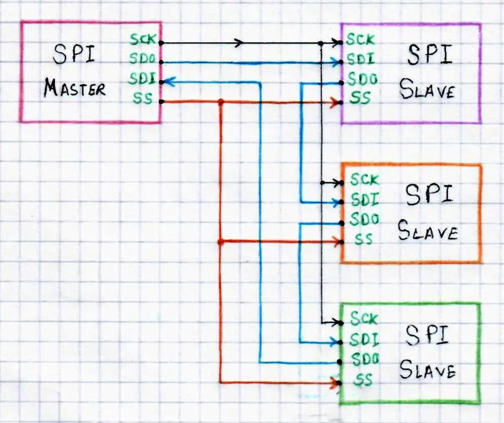
The master device can select which slave to talk to by setting the SS (slave select) pin to logic low. If a single slave is being addressed, you can tie the SS pin of this slave device to logic low without the need to control this line by the master.
Clock Rate (At The Master End)
The Master device on the SPI bus has to configure and generate the clock signal at the beginning of any communication. During each SPI clock cycle, full-duplex data transmission occurs. The master sends a bit on the MOSI line and the slave reads it, while the slave sends a bit on the MISO line and the master reads it.
This sequence is maintained even when only one-directional data transfer is intended. Which means in order to receive any data you have to actually send something! in this case, we call it “Dummy Data” or “Junk”!
Theoretically, the clock rate can be whatever you want provided that it’s practically realizable. The SPI serial clock is derived from the CLKsys of your system, which means it can by Fosc/2 or 4, 8, 16 or whatever. The dynamic range starts from a few KHz up to several MHz. (Practical limitations are case-dependent for each system).
Clock Polarity – CKP
Besides configuring the serial clock rate (frequency), the SPI Master device should also configure the clock polarity. The clock polarity is usually written as CKP or CPOL depending on the hardware manufacturer but in the end, it’s the same. The clock polarity & phase together determine when will the data be latched on the data line.
CKP can be configured to be 1 or 0. Which means you can set the default state of the clock (the IDLE) to be high or low whichever you want. The polarity inversion can be achieved by a simple logic inverter. You have to refer to the device’s datasheet in order to set both CKP & CKE properly.
- For (CKP = 0), the clock IDLEs at 0, and each cycle consists of a pulse of 1. That is, the leading edge is a rising edge, and the trailing edge is a falling edge.
- For (CKP = 1), the clock IDLEs at 1, and each cycle consists of a pulse of 0. That is, the leading edge is a falling edge, and the trailing edge is a rising edge.
Clock Phase (Edge) – CKE
Besides configuring the serial clock rate and polarity, the SPI Master device should also configure the clock phase (or Edge). The clock phase is usually written as CKE or CPHA depending on the hardware manufacturer but in the end, it’s the same. The clock polarity & phase together determine when will the data be latched on the data line.
CKE can be configured to be 1 or 0. Which means you can set the edge on which the data will be latched whether it’s a rising or falling edge (leading or trailing). You have to refer to the device’s datasheet in order to set both CKP & CKE properly.
- For (CKE = 0), the “out” side changes the data on the trailing edge of the preceding clock cycle, while the “in” side captures the data on (or shortly after) the leading edge of the clock cycle.
- For (CKE = 1), the “out” side changes the data on the leading edge of the current clock cycle, while the “in” side captures the data on (or shortly after) the trailing edge of the clock cycle.
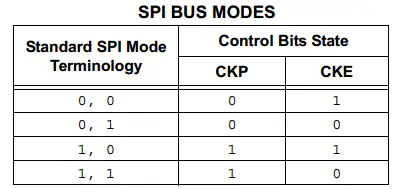
SPI Clock Configurations Summary
The clock phase and the polarity together control whether the data is latched on the rising or falling edge (CKE) as well as the IDLE state of the clock (CKP). The diagram below summarizes all the clock configuration combinations and highlighting when the data is actually latched.
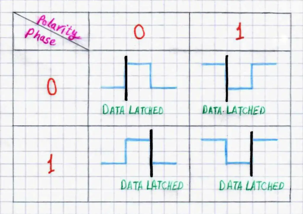
As you might have noticed, if the SPI Master doesn’t configure the CKP (clock polarity) & CKE (clock phase) to what the slave device expects, any sort of communication (write/read) will fail.
Mode Numbers
The combination of both clock polarity and phase is commonly referred to as “SPI Mode”. All the possible modes are numbered following the convention down below.
| SPI Mode | Clock Polarity
(CKP/CPOL) |
Clock Phase
(CPHA) |
Clock Edge
(CKE/NCPHA) |
| 0 [00] | 0 | 0 | 1 |
| 1 [01] | 0 | 1 | 0 |
| 2 [10] | 1 | 0 | 1 |
| 3 [11] | 1 | 1 | 0 |
[Note that: NCPHA is the inversion of CPHA signal]. The above table shows the SPI mode numbers for Microchip PIC and ARM-Core Based Microcontrollers. Other microcontrollers follow the convention below
| SPI Mode | CPOL | CPHA |
| 0 [00] | 0 | 0 |
| 1 [01] | 0 | 1 |
| 2 [10] | 1 | 0 |
| 3 [11] | 1 | 1 |
You should also double-check the modes table included in the microcontroller’s datasheet to make sure everything is OK.
SPI Bus Configurations
All devices on the SPI bus including the master and all slaves can all be connected in a couple of different configurations. Which mostly depend on how they are manufactured and how data should be flowing through the network of devices in that particular application. I’ll briefly describe both of these configurations hereafter.
Daisy Chain

In the digital communication world, when devices are connected together in such a way that data has to circulate between devices until it reaches destination device, it’s then called a Daisy Chain!
Each device is connected between 2 other devices in a circular (Logically) way as shown in the diagram down below. [note that: a logical circle is a term that describes data circulation flow in the network which means that devices connection doesn’t necessarily need to be circular in shape].
The SPI port of each slave device is designed to send data out during the second group of clock pulses an exact copy of the data it received during the first group of clock pulses. The whole chain acts as a communication shift register. Each slave copies the input data to the output in the next clock cycle until the SS line goes high. Such a feature only requires a single SS line from the master, rather than a separate SS line for each slave.
That means a data frame will keep propagating through slave devices as long as the SS line is held low. The following diagram will show you how a single SPI master can address multiple slave devices using only one SS line.
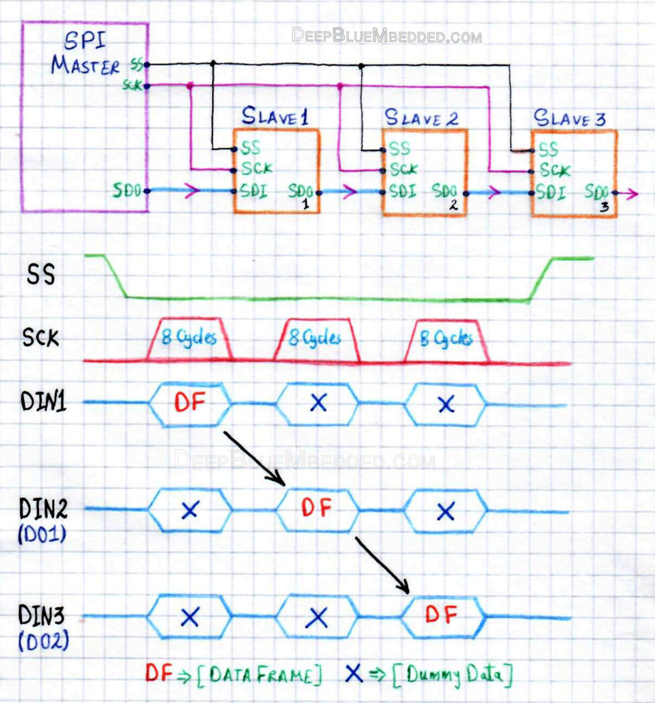
And that’s it for the daisy chain SPI bus configuration. Now, we’ll turn over to see the other configuration which we’ll be actually implementing before the end of this tutorial.
Independent Slave
In the independent slave configuration, there is an independent slave select line for each slave. This is the way SPI is normally used. The master asserts only one chip select at a time. Since the SDO/SDI pins of the slaves are connected together, they are required to be tri-state logic pins. Slave devices which don’t support tri-state may be used in independent slave configuration by adding a tri-state buffer chip controlled by the chip select signal.
A typical connection diagram for a system with multiple slaves connected in the independent configuration is shown below.
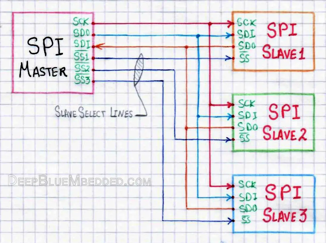
As you can see, this configuration can be impractical in case your system involves many SPI slave devices. Which will require too many IO pins to control all SS lines.
Advantages of SPI Communication
There are many reasons that make SPI stands out as a serial communication interface. Here is a short list for the pros of SPI.
- Full-Duplex serial communication.
- Potentially high-speed data transfer rates can be achieved with SPI.
- Few wires are required for the SPI Bus (typically 4 lines).
- Easy software configuration and setup.
- Extremely flexible data transfer. It’s not limited to 8-Bits, it can be any arbitrarily-sized words.
- Very simple hardware structure. Slaves don’t need unique addresses (unlike I2C). Slaves use the master’s clock and do not need precision oscillators (unlike UART). Transceivers are not needed (unlike CAN).
Disadvantages of SPI
- No hardware slave acknowledgment (the master could be transmitting to nowhere without knowing).
- Typically supports only one master device.
- Requires more pins (unlike I2C).
- No hardware-level error-checking protocol is defined.
- Many existing variations and conventions make it ambiguous sometimes and you’ve to dig very deep in the datasheet and underline every single word.
- Can only support very short distances (usually onboard communications) compared to RS-232 and CAN-Bus.
SPI In PIC16F87X Microcontrollers
Description
Microchip PIC microcontrollers do have a hardware module called “MSSP” which is an acronym for “Master Synchronous Serial Port”. The MSSP module can operate in one of two modes:
• Serial Peripheral Interface (SPI)
• Inter-Integrated Circuit (I2C)
– Full Master mode
– Slave mode (with general address call)
Which means that we need to configure this module in order to have it operating as an SPI or I2C interface. And that’s the goal of this tutorial, to see how can we set up the MSSP module to operate as a slave or a master.
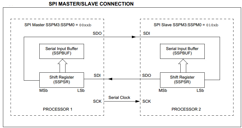
The SPI mode allows 8 bits of data to be synchronously transmitted and received simultaneously. All four modes of SPI are supported. To accomplish communication, typically three pins are used:
• Serial Data Out (SDO) –> RC5/SDO
• Serial Data In (SDI) –> RC4/SDI/SDA
• Serial Clock (SCK) –> RC3/SCK/SCL
Additionally, a fourth pin may be used when in a Slave mode of operation:
• Slave Select (SS) –> RA5/AN4/SS/C2OUT
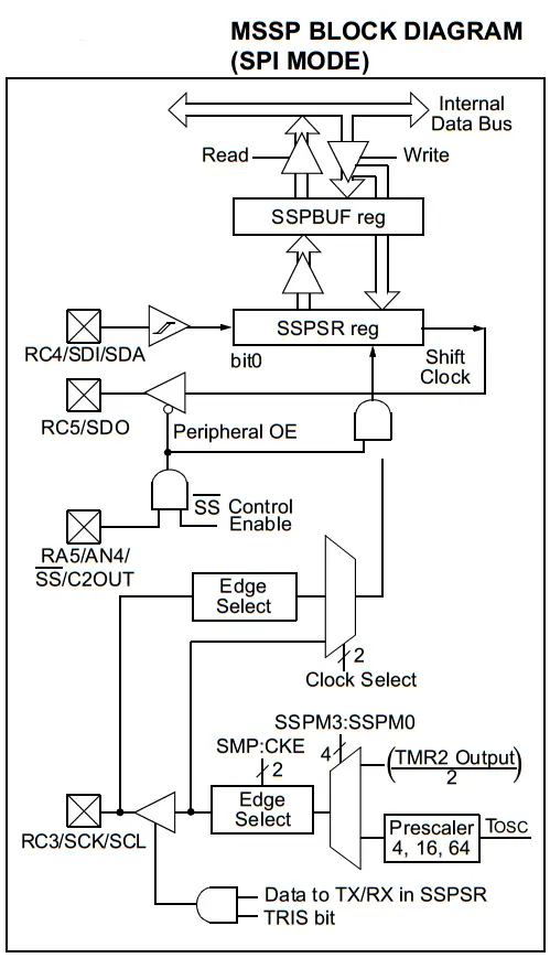
The figure below shows the functional logic diagram of the hardware MSSP module (in SPI Mode).
SPI Operation
When initializing the SPI, several options need to be specified. This is done by programming the appropriate control bits [ SSPCON<5:0> & SSPSTAT<7:6> ]. These control bits allow the following configurations to be specified:
• Master mode (SCK is the clock output)
• Slave mode (SCK is the clock input)
• Clock Polarity – CKP (Idle state of SCK)
• Data Input Sample Phase – SMB (middle or end of data output time)
• Clock Edge – CKE (output data on the rising/falling edge of SCK)
• Clock Rate (Master mode only)
• Slave Select mode (Slave mode only)
The MSSP consists of a transmit/receive shift register (SSPSR) and a buffer register (SSPBUF). The SSPSR shifts the data in and out of the device, MSB first. The SSPBUF holds the data that was written to the SSPSR until the received data is ready. Once the eight bits of data have been received, that byte is moved to the SSPBUF register. Then, the Buffer Full detect bit, BF (SSPSTAT<0>), and the interrupt flag bit, SSPIF, are set. This double-buffering of the received data (SSPBUF) allows the next byte to start reception before reading the data that was just received.
Any write to the SSPBUF register during transmission/reception of data will be ignored and the write collision detects bit, WCOL (SSPCON<7>), will be set. User software must clear the WCOL bit so that it can be determined if the following write(s) to the SSPBUF register completed successfully. When the application software is expecting to receive valid data, the SSPBUF should be read before the next byte of data to transfer is written to the SSPBUF. Buffer Full bit, BF (SSPSTAT<0>), indicates when SSPBUF has been loaded with the received data (transmission is complete). When the SSPBUF is read, the BF bit is cleared. This data may be irrelevant if the SPI is only a transmitter.
Generally, the MSSP interrupt is used to determine when the transmission/reception has completed. The SSPBUF must be read and/or written. If the interrupt method is not going to be used, then software polling can be done to ensure that a write collision does not occur.
The SSPSR is not directly readable or writable and can only be accessed by addressing the SSPBUF register. Additionally, the MSSP Status register (SSPSTAT) indicates the various status conditions.
SPI IO Pin Configurations
To enable the MSSP serial port, the SSP Enable bit, SSPEN (SSPCON<5>), must be set. To reset the MSSP or reconfigure SPI mode, clear the SSPEN bit, re-initialize the SSPCON registers and then set the SSPEN bit. This is done for SPI mode switching or in order to initiate I2C communication. This configures the SDI, SDO, SCK and SS pins as serial port pins. For the pins to behave as the serial port function, some must have their data direction bits (in the TRISx register) appropriately programmed. That is:
• SDI => is automatically controlled by the SPI module
• SDO => must have TRISC<5> bit cleared
• SCK => (Master mode) must have TRISC<3> bit cleared
• SCK => (Slave mode) must have TRISC<3> bit set
• SS => must have TRISC<4> bit set
Any serial port function that is not desired may be overridden by programming the corresponding data direction (TRISx) register to the opposite value.
SPI Typical Connection
The diagram below shows a typical SPI Bus connection between two MCUs. The master controller (Processor 1) initiates the data transfer by sending the SCK signal. Data frame is shifted out of both shift registers on their programmed clock edge and latched on the opposite edge of the clock. Both processors should be programmed to the same Clock Polarity (CKP), then both controllers would send and receive data at the same time. Whether the data frame is meaningful (or dummy data) depends on the application software. which means there are three possible scenarios for SPI data transaction:
• Master sends a Data Frame – Slave sends Dummy Data
• Master sends a Data Frame – Slave sends another Data Frame
• Master sends Dummy Data – Slave sends a Data Frame
SPI Bus Modes in PIC vs Standards
The Table down below (From PIC16F87X Datasheet) shows the compatibility between the standard SPI modes and the states of the CKP and CKE control bits. Additionally, There is also an SMP bit which controls when the data is sampled, and it has no effect of the SPI mode number in fact.
SPI – Master Mode
The SPI Master can initiate the data transfer at any time because it controls the SCK. The master determines when the slave is to broadcast data by the software protocol.
In Master mode, the data is transmitted/received as soon as the SSPBUF register is written to. If the SPI is only going to receive, the SDO output could be disabled (programmed as an input). The SSPSR register will continue to shift in the signal present on the SDI pin at the programmed clock rate.
As each byte is received, it will be loaded into the SSPBUF register as if a normally received byte (interrupts and status bits appropriately set). And it’s up to the programmers (you and me) to choose whether to poll the status bits or to use the interrupt signals.
The clock phase and polarity are selected by appropriately programming the control bits. This then would give waveforms for SPI communication as shown in the timings diagram down below.
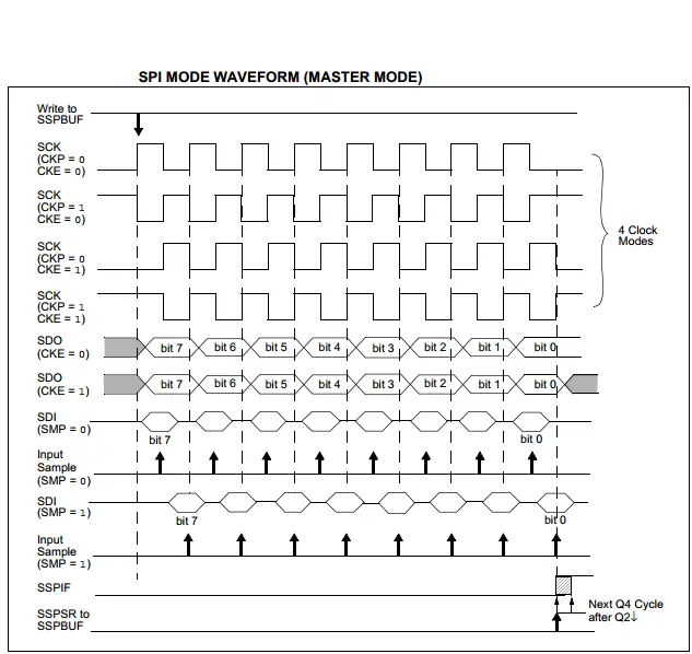
In Master mode, the SPI clock rate (bit rate) is user programmable to be one of the following:
• FOSC/4 (or TCY)
• FOSC/16 (or 4 • TCY)
• FOSC/64 (or 16 • TCY)
• Timer2 output/2
This allows a maximum data transfer rate (at Fosc = 40 MHz) of 10.00 Mbps.
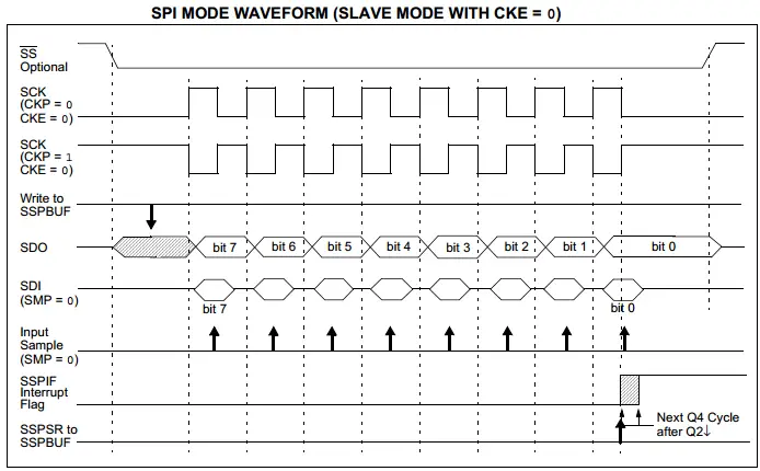
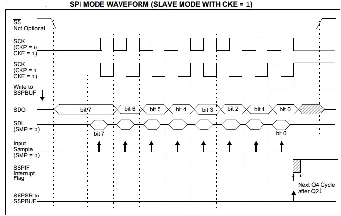
SPI – Slave Mode
In Slave mode, the data is transmitted and received as the external clock pulses appear on SCK. When the last bit is latched, the SSPIF interrupt flag bit is set.
While in Slave mode, the external clock is supplied by the external clock source on the SCK pin. This external clock must meet the minimum high and low times as specified in the electrical specifications.
While in Sleep mode, the slave can transmit/receive data. When a byte is received, the device will wake-up from Sleep.
The SS pin allows a Synchronous Slave mode. The SPI must be in Slave mode with SS pin control enabled. The pin must not be driven low for the SS pin to function as an input. The data latch must be high. When the SS pin is low, transmission and reception are enabled and the SDO pin is driven.
When the SS pin goes high, the SDO pin is no longer driven even if in the middle of a transmitted byte and becomes a floating output. Any running/further SPI communication will be aborted. External pull-up/pull-down resistors may be desirable, depending on the application. The diagram down below shows the Slave Synchronization Waveforms & The Effect of pulling the SS pin to logic High (Note: that communication is suspended while SS is held high).
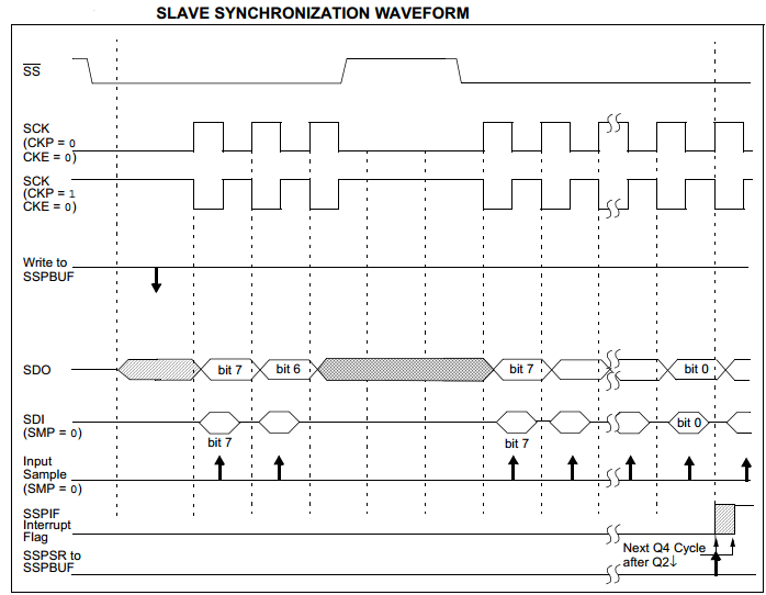
The clock phase and polarity are selected by appropriately programming the control bits. This then would give waveforms for SPI communication (in Slave Mode) as shown in the timings diagrams down below.
SPI SFR Registers
The MSSP module has four registers for SPI mode operation. These are
- MSSP Control Register (SSPCON)
- MSSP Status Register (SSPSTAT)
- Serial Receive/Transmit Buffer Register (SSPBUF)
- MSSP Shift Register (SSPSR) – Not directly accessible
SSPCON & SSPSTAT
SSPCON and SSPSTAT are the control and status registers in SPI mode operation. The SSPCON register is readable and writable. The SPI hardware is configured by programming the appropriate bits of this couple of registers. The exact available options are indicated in the register table hereafter in the text (exactly as is in the datasheet).
SSPSR & SSPBUF
SSPSR is the shift register used for shifting data in or out. SSPBUF is the buffer register to which data bytes are written to or read from. In receive operations, SSPSR and SSPBUF together create a double-buffered receiver. When SSPSR receives a complete byte, it is transferred to SSPBUF and the SSPIF interrupt is set. During transmission, the SSPBUF is not double-buffered. A write to SSPBUF will write to both SSPBUF and SSPSR.
 SSPSTAT – MSSP Status Register (SPI Mode)
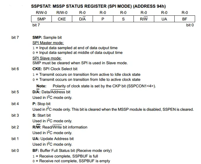
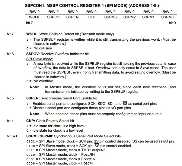
SSPCON1 – MSSP Control Register 1 (SPI Mode)
How To Configure An SPI Master?
In this section, we’ll be focusing on the process of configuring a PIC microcontroller to work as an SPI Master. Enough of general information about SPI. Let’s get our microcontroller to work as a serial SPI Master (transmitter)!
The Mechanics of SPI Transmission
| The SPI Master initiates communication when a data frame (Byte) is written to the buffer register SSPBUF. The SPI hardware will generate an SCK signal with the appropriate configurations and shifts out the data which was latched from the SSPBUF to the SSPSR shift register. The MSb is shifted out first followed by the rest of the 8-bit data frame. When the data (byte) is successfully transmitted, an interrupt signal is generated which may help you for starting or waiting before another data transaction process. You can now easily identify this functionality by carefully following the SPI hardware block diagram.
If it looks overwhelming, stay cool. It really does! Each of us has been at the same point and yes! it felt overwhelming. Take the time to understand each step of it. Down below are the exact brief steps that you should follow to configure your SPI Master, even without looking up any diagram in the datasheet. However, you should consider doing so sooner or later at some point. |
|
Steps For Configuring SPI Master
| 1 | Set The SPI Mode (to Master), and Set the desired Clock Rate for SCK by programming the (SSPM3:SSPM0) Bits [In Register SSPCON1<3:0>]. |
| 2 | Enable The Synchronous Serial Port by setting the SSPEN bit. |
| 3
|
Configure the Serial Clock Polarity & Phase by programming both CKP, CKE bits.
|
| 4 | Configure when the input data is sampled (at the end or middle of data output time) by programming the SMP bit [Register SSPSTAT<7>]. |
| 5
|
Configure the IO pins which will be used by the SPI hardware for master mode by writing to the corresponding bits in TRISx register.
|
| 6 | Enable SPI Reception Interrupts, if needed and it’s highly recommended, by setting (SSPIE, PEIE, and GIE). |
| 7 | Read The Data From SSPBUF Register. This step clears the BF bit. And don’t also forget to clear the interrupt flag bit SSPIF after reading the received data from the buffer. |
Implementing SPI Master Driver Firmware
Step1 Set The SPI Mode (to Master), and Set the desired Clock Rate
|
1 2 3 4 5 |
// Set Spi Mode To Master + Set SCK Rate To Fosc/64 SSPM0 = 0; SSPM1 = 0; SSPM2 = 0; SSPM3 = 0; |
Step2 Enable The Synchronous Serial Port
|
1 |
SSPEN = 1; |
Step3 Configure the Serial Clock Polarity & Phase
|
1 2 3 |
// Configure The Clock Polarity & Phase (SPI Mode Num. 1) CKP = 0; CKE = 0; |
Step4 Configure when the input data is sampled
|
1 |
SMP = 0; // (At The Middle) |
Step5 Configure the IO pins For SPI Master Mode
|
1 2 3 |
TRISC5 = 0; // SDO -> Output TRISC4 = 1; // SDI -> Input TRISC3 = 0; // SCK -> Output |
Step6 Enable SPI Transmission Interrupts (if needed)
|
1 2 3 |
SSPIE = 1; PEIE = 1; GIE = 1; |
SPI Master Full Code Listing
You can easily use those 2-functions within your code. Calling the SPI_Master_Init() procedure will configure the SPI as a Master for you. Then, calling the SPI_Write(data) will shift-out the data frame from your transmitter to the receiving end.
|
1 2 3 4 5 6 7 8 9 10 11 12 13 14 15 16 17 18 19 20 21 22 23 24 25 26 27 28 29 |
void SPI_Master_Init() { // Set SPI Mode To Master + Set SCK Rate To Fosc/64 SSPM0 = 0; SSPM1 = 0; SSPM2 = 0; SSPM3 = 0; // Enable The Synchronous Serial Port SSPEN = 1; // Configure The Clock Polarity & Phase (SPI Mode Num. 1) CKP = 0; CKE = 0; // Configure The Sampling Time (Let's make it at middle) SMP = 0; // Configure The IO Pins For SPI Master Mode TRISC5 = 0; // SDO -> Output TRISC4 = 1; // SDI -> Input TRISC3 = 0; // SCK -> Output // If Interrupts Are Needed, Un-comment The Line Below // SSPIE = 1; PEIE = 1; GIE = 1; } void SPI_Write(uint8_t Data) { SSPBUF = Data; // Transfer The Data To The Buffer Register // while(!BF); // Un-comment it if you're Not Using Interrupts! // The Above While Loop Protects Against Writing To The Buffer Before // The Previous Transmission Ends } |
How To Configure An SPI Slave?
In this section, we’ll be discussing the process of configuring a PIC microcontroller to work as an SPI Slave. And develop the necessary firmware code step-by-step.
The Mechanics of SPI Reception
| The SPI Master shifts the data out of its SSPSR register, MSb first. The SSPSF at the slave is simultaneously receiving the exact same bits being shifted out of the master device. Once the eight bits of data have been received, the byte is then moved to the SSPBUF register. Then, the Buffer Full detect bit, BF (SSPSTAT<0>), and the interrupt flag bit, SSPIF, are set. This double-buffering of the received data (SSPBUF) allows the next byte to start reception before reading the data that was just received.
Down below are the exact brief steps that you should follow to configure your SPI Master, even without looking up any diagram in the datasheet. However, you should consider doing so sooner or later at some point.
|
|
Steps For Configuring SPI Slave
| 1 | Set The SPI Mode (to Slave + SS Enabled) by programming the (SSPM3:SSPM0) Bits [In Register SSPCON1<3:0>]. |
| 2 | Enable The Synchronous Serial Port by setting the SSPEN bit. |
| 3
|
Configure the Serial Clock Polarity & Phase by programming both CKP, CKE bits. [Same As Master]
|
| 4 | Clear the SMP bit [Register SSPSTAT<7>]. |
| 5
|
Configure the IO pins which will be used by the SPI hardware for slave mode by writing to the corresponding bits in TRISx register.
|
| 6 | Enable SPI Transmission Interrupts, it’s highly recommended, by setting (SSPIE, PEIE, and GIE). |
| 7 | Read The Received Data From the SSPBUF Register. This step clears the BF bit. Don’t also forget to clear the interrupt flag bit SSPIF after reading the SSPBUF register. |
Implementing SPI Slave Driver Firmware
Step1 Set The SPI Mode (to Slave + SS Enabled)
|
1 2 3 4 5 |
// Set SPI Mode To Slave + SS Enabled SSPM0 = 0; SSPM1 = 0; SSPM2 = 1; SSPM3 = 0; |
Step2 Enable The Synchronous Serial Port
|
1 |
SSPEN = 1; |
Step3 Configure the Serial Clock Polarity & Phase
|
1 2 3 |
// Configure The Clock Polarity & Phase (SPI Mode Num. 1) CKP = 0; CKE = 0; |
Step4 Clear The SMP Bit
|
1 |
SMP = 0; // (as stated in the datasheet) |
Step5 Configure the IO pins For SPI Master Mode
|
1 2 3 4 5 6 7 8 |
TRISC5 = 0; // SDO -> Output TRISC4 = 1; // SDI -> Input TRISC3 = 1; // SCK -> Intput PCFG3 = 0; // Set SS (RA5/AN4) To Be Digital IO PCFG2 = 1; PCFG1 = 0; PCFG0 = 0; TRISA5 = 1; // SS -> Input |
Step6 Enable SPI Reception Interrupts (Highly Recommended)
|
1 2 3 |
SSPIE = 1; PEIE = 1; GIE = 1; |
SPI Slave Full Code Listing
You can easily use those functions within your code. Calling the SPI_Slave_Init() procedure will configure the SPI Slave for you. Then, calling the SPI_Read() will return the data frame from your receiver buffer register. It’s not recommended to poll the SPI BF buffer filled status bit. The best way is to use interrupt signals.
|
1 2 3 4 5 6 7 8 9 10 11 12 13 14 15 16 17 18 19 20 21 22 23 24 25 26 27 28 29 30 31 32 33 34 35 36 37 38 39 40 41 42 43 44 45 46 47 48 49 50 |
void SPI_Slave_Init() { // Set Spi Mode To Slave + SS Enabled SSPM0 = 0; SSPM1 = 0; SSPM2 = 1; SSPM3 = 0; // Enable The Synchronous Serial Port SSPEN = 1; // Configure The Clock Polarity & Phase (SPI Mode Num. 1) CKP = 0; CKE = 0; // Clear The SMP Bit SMP = 0; // Configure The IO Pins For SPI Master Mode TRISC5 = 0; // SDO -> Output TRISC4 = 1; // SDI -> Input TRISC3 = 1; // SCK -> Intput PCFG3 = 0; // Set SS (RA5/AN4) To Be Digital IO PCFG2 = 1; PCFG1 = 0; PCFG0 = 0; TRISA5 = 1; // SS -> Input // Enable Interrupts. Comment Them To Disable interrupts(NOT Recommended) SSPIE = 1; PEIE = 1; GIE = 1; } uint8_t SPI_Read() { uint8_t Data; if(BF) // Check If Any New Data Is Received { Data = SSPBUF; // Read The Buffer BF = 0; // Clear The Buffer-Filled Indicator Bit SSPIF = 0; // Clear The Interrupt Flag Bit SSPOV = 0; // Clear The Overflow Indicator Bit return Data; } } void __interrupt ISR(void) { if(SSPIF) { Data = SSPBUF; // Read The Buffer SSPIF = 0; // Clear The Interrupt Flag } } |
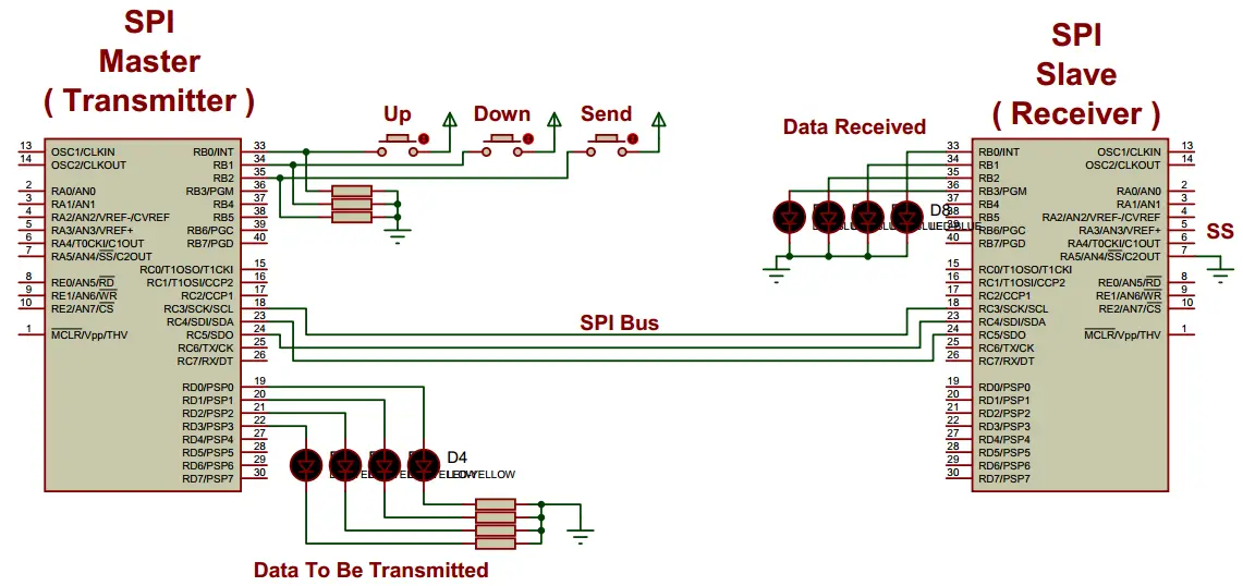
µC-To-µC SPI Communication – LAB
| Lab Name | SPI Basic Communication |
| Lab Number | 20 |
| Lab Level | Intermediate |
| Lab Objectives | Learn how to create a serial communication interface between 2 microcontrollers using SPI Protocol. We’ll send specific data frames from a transmitter MCU and receive it back with another one then double-check the data correctness and validate the communication process. |
1. Coding
Open the MPLAB IDE and create a couple of new projects name them “SPI_Master” and “SPI_Slave” for master and slave MCUs respectively. If you have some issues doing so, you can always refer to the previous tutorial using the link below.

Set the configuration bits to match the generic setting which we’ve stated earlier. And if you also find troubles creating this file, you can always refer to the previous tutorial using the link below.

Now, open the main.c file of each project and let’s start developing the firmware for our project.
1. SPI Transmitter (Master)
[ Transmitter Firmware ]
Our task is to take 3 inputs from the user using 3 push buttons to do the following tasks:
Button1: increment the data value
Button2: decrement the data value
Button3: send the current data frame via SPI
We’ll use PORTD to display the current data value for the user. And 3 input pins of PORTB. Obviously, we’ll also configure our microcontroller to operate as a transmitter as we’ve seen earlier in this tutorial. Here is the full code listing for the transmitter MCU chip.
|
1 2 3 4 5 6 7 8 9 10 11 12 13 14 15 16 17 18 19 20 21 22 23 24 25 26 27 28 29 30 31 32 33 34 35 36 37 38 39 40 41 42 43 44 45 46 47 48 49 50 51 52 53 54 55 56 57 58 59 60 61 62 63 64 65 66 67 68 69 70 71 72 73 74 75 76 77 78 79 80 81 82 83 84 85 |
/* * LAB Number: 20 * LAB Name: SPI_Basic_Communication (Master Code) * Author: Khaled Magdy * For More Information Visit My Website @ DeepBlueMbedded.com * */ #include <xc.h> #include <stdint.h> #include "config.h" #define _XTAL_FREQ 4000000 //-------------------------------- // IO Pins Defines (Mappings) #define UP RB0 #define Down RB1 #define Send RB2 //-------------------------------- // Functions Declarations void SPI_Master_Init(); void SPI_Write(uint8_t); //-------------------------------- // Main Routine void main(void) { //--[ Peripherals & IO Configurations ]-- SPI_Master_Init(); // Initialize The SPI in Master Mode @ Fosc/64 SCK uint8_t Data = 0; // The Data Byte TRISB = 0x07; // RB0, RB1 & RB2 Are Input Pins (Push Buttons) TRISD = 0x00; // Output Port (4-Pins) PORTD = 0x00; // Initially OFF //--------------------------- while(1) { if (UP) // Increment The Data Value { Data++; __delay_ms(250); } if (Down) // Decrement The Data Value { Data--; __delay_ms(250); } if (Send) // Send The Current Data Value Via SPI { SPI_Write(Data); __delay_ms(250); } PORTD = Data; // Display The Current Data Value @ PORTD } return; } //------------------------------- // Functions Definitions void SPI_Master_Init() { // Set Spi Mode To Master + Set SCK Rate To Fosc/64 SSPM0 = 0; SSPM1 = 0; SSPM2 = 0; SSPM3 = 0; // Enable The Synchronous Serial Port SSPEN = 1; // Configure The Clock Polarity & Phase (SPI Mode Num. 1) CKP = 0; CKE = 0; // Configure The Sampling Time (Let's make it at middle) SMP = 0; // Configure The IO Pins For SPI Master Mode TRISC5 = 0; // SDO -> Output TRISC4 = 1; // SDI -> Input TRISC3 = 0; // SCK -> Output // If Interrupts Are Needed, Un-comment The Line Below // SSPIE = 1; PEIE = 1; GIE = 1; } void SPI_Write(uint8_t Data) { SSPBUF = Data; // Transfer The Data To The Buffer Register // while(!SSPSTATbits.BF); // Un-comment it if you're Not Using Interrupts! // The Above While Loop Protects Against Writing To The Buffer // Before The Previous Transmission Ends } |
2. SPI Receiver (Slave)
[ Receiver Firmware ]
Our task is to set up the SPI module to operate in slave mode and enable the SPI data reception interrupt. Within the ISR handler, we should read the received byte of data and latch it out to PORTB with some LEDs for data inspection. And here is the full code listing for the receiver MCU chip.
|
1 2 3 4 5 6 7 8 9 10 11 12 13 14 15 16 17 18 19 20 21 22 23 24 25 26 27 28 29 30 31 32 33 34 35 36 37 38 39 40 41 42 43 44 45 46 47 48 49 50 51 52 53 54 55 56 57 58 59 60 61 62 63 64 65 66 67 68 69 70 71 72 73 74 75 76 77 78 79 80 |
/* * LAB Number: 20 * LAB Name: SPI_Basic_Communication (Slave Code) * Author: Khaled Magdy * For More Information Visit My Website @ DeepBlueMbedded.com * */ #include <xc.h> #include <stdint.h> #include "config.h" void SPI_Slave_Init(); uint8_t SPI_Read(); uint8_t Data; // Global Received Data Variable (Not Recommended) // Just For Demonstration Purposes Only! void main(void) { SPI_Slave_Init(); TRISB = 0x00; while(1) { // Dumping Received Data To PORTB To Validate Communication Success! PORTB = Data; } return; } void SPI_Slave_Init() { // Set Spi Mode To Slave + SS Enabled SSPM0 = 0; SSPM1 = 0; SSPM2 = 1; SSPM3 = 0; // Enable The Synchronous Serial Port SSPEN = 1; // Configure The Clock Polarity & Phase (SPI Mode Num. 1) CKP = 0; CKE = 0; // Clear The SMP Bit SMP = 0; // Configure The IO Pins For SPI Master Mode TRISC5 = 0; // SDO -> Output TRISC4 = 1; // SDI -> Input TRISC3 = 1; // SCK -> Intput PCFG3 = 0; // Set SS (RA5/AN4) To Be Digital IO PCFG2 = 1; PCFG1 = 0; PCFG0 = 0; TRISA5 = 1; // SS -> Input // Enable Interrupts. Comment Them To Disable interrupts(NOT Recommended) SSPIE = 1; PEIE = 1; GIE = 1; } uint8_t SPI_Read() // Not Recommended Method To Read SPI Data { uint8_t Data; if(BF) // Check If Any New Data Is Received { Data = SSPBUF; // Read The Buffer BF = 0; // Clear The Buffer-Filled Indicator Bit SSPIF = 0; // Clear The Interrupt Flag Bit SSPOV = 0; // Clear The Overflow Indicator Bit return Data; } } void __interrupt ISR(void) { if(SSPIF) { Data = SSPBUF; // Read The Buffer SSPIF = 0; // Clear The Interrupt Flag } } |
And We’re Done With The Firmware! Cross Your Fingers! And Hit The Compile Button!
2. Simulation
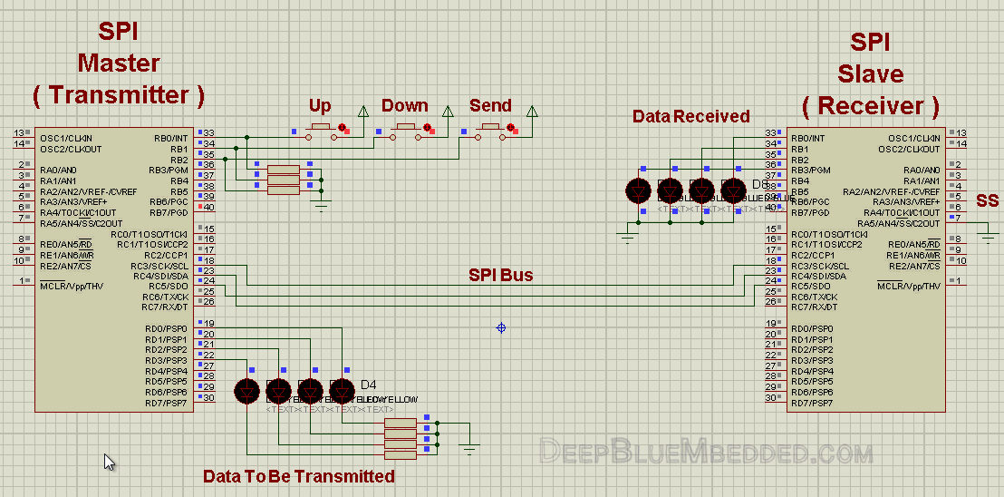
Create the simulation project on your simulator and connect your circuitry as shown in the schematic diagram down below. Add the hex code to the respective microcontroller chip. The receiver code to the receiver chip and so. Click the run button and test out everything!
The Running Simulation Test!
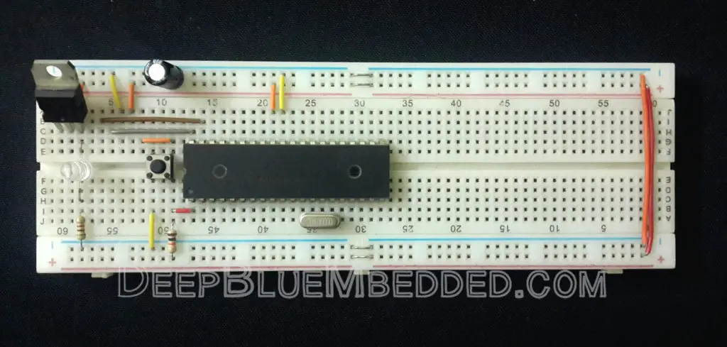
3. Prototyping
If you’ve correctly followed the schematics shown above in the simulation section, you should get your code up and running on a real breadboard flawlessly! However, you should be careful with grounding and connections and make sure that you’ve (flashed) uploaded the right code to each chip (Master & Slave).
And here is the final running prototype for this project in case you’re curious.
 |
4. Firmware Template
The previous code listings for this lab despite being fully-functional. It may need a little bit of work to get it working at a different data rate or in another SPI mode number. That’s why I’ll give you a template for more portable and easier to use firmware for both your transmitter & receiver devices.
Transmitter ( Master Code )
|
1 2 3 4 5 6 7 8 9 10 11 12 13 14 15 16 17 18 19 20 21 22 23 24 25 26 27 28 29 30 31 32 33 34 35 36 37 38 39 40 41 42 43 44 45 46 47 48 49 50 51 52 53 54 55 56 57 58 59 60 61 62 63 64 65 66 67 68 69 70 |
/* * File Name: SPI Firmware Template For (Master / Transmitter) * Author: Khaled Magdy * For More Information Visit My Website @ DeepBlueMbedded.com * */ #include <xc.h> #include <stdint.h> #include "config.h" #define _XTAL_FREQ 4000000 //-------------------------------- // Functions Declarations void SPI_Master_Init(void); void SPI_Write(uint8_t); void SPI_Write_String(char *); //-------------------------------- // Main Routine void main(void) { //--[ Peripherals & IO Configurations ]-- SPI_Master_Init(); // Initialize The SPI in Master Mode @ Fosc/64 //--------------------------- while(1) { // Do Whatever You Want ! // ... } return; } //-------------------------------- // Functions Definitions void SPI_Master_Init() { // Set Spi Mode To Master + Set SCK Rate To Fosc/64 SSPM0 = 0; SSPM1 = 0; SSPM2 = 0; SSPM3 = 0; // Enable The Synchronous Serial Port SSPEN = 1; // Configure The Clock Polarity & Phase (SPI Mode Num. 1) CKP = 0; CKE = 0; // Configure The Sampling Time (Let's make it at middle) SMP = 0; // Configure The IO Pins For SPI Master Mode TRISC5 = 0; // SDO -> Output TRISC4 = 1; // SDI -> Input TRISC3 = 0; // SCK -> Output // If Interrupts Are Needed, Un-comment The Line Below // SSPIE = 1; PEIE = 1; GIE = 1; } void SPI_Write(uint8_t Data) { SSPBUF = Data; // Transfer The Data To The Buffer Register // while(!SSPSTATbits.BF); // Un-comment it if you're Not Using Interrupts! // The Above While Loop Protects Against Writing To The Buffer // Before The Previous Transmission Ends } void SPI_Write_String(char *text) { uint16_t i; for(i=0;text[i]!='\0';i++) SPI_Write(text[i]); } |
Receiver ( Slave Code )
|
1 2 3 4 5 6 7 8 9 10 11 12 13 14 15 16 17 18 19 20 21 22 23 24 25 26 27 28 29 30 31 32 33 34 35 36 37 38 39 40 41 42 43 44 45 46 47 48 49 50 51 52 53 54 55 56 57 58 59 60 61 62 63 64 65 66 67 68 69 70 71 72 73 74 75 76 77 78 79 80 81 82 83 84 85 86 87 88 89 90 91 |
/* * File Name: SPI Firmware Template For (Slave / Receiver) * Author: Khaled Magdy * For More Information Visit My Website @ DeepBlueMbedded.com * */ #include <xc.h> #include <stdint.h> #include "config.h" #define _XTAL_FREQ 4000000 //-------------------------------- // Functions Declarations void SPI_Slave_Init(); uint8_t SPI_Read(); void SPI_Read_String(uint8_t *, uint16_t); //-------------------------------- // Main Routine void main(void) { //--[ Peripherals & IO Configurations ]-- SPI_Slave_Init(); // Initialize The SPI in Master Mode @ Fosc/64 //--------------------------- while(1) { // Do Whatever You Want ! // ... } return; } //-------------------------------- // Functions Definitions void SPI_Slave_Init() { // Set Spi Mode To Slave + SS Enabled SSPM0 = 0; SSPM1 = 0; SSPM2 = 1; SSPM3 = 0; // Enable The Synchronous Serial Port SSPEN = 1; // Configure The Clock Polarity & Phase (SPI Mode Num. 1) CKP = 0; CKE = 0; // Clear The SMP Bit SMP = 0; // Configure The IO Pins For SPI Master Mode TRISC5 = 0; // SDO -> Output TRISC4 = 1; // SDI -> Input TRISC3 = 1; // SCK -> Intput PCFG3 = 0; // Set SS (RA5/AN4) To Be Digital IO PCFG2 = 1; PCFG1 = 0; PCFG0 = 0; TRISA5 = 1; // SS -> Input // Enable Interrupts. Comment Them To Disable interrupts(NOT Recommended) SSPIE = 1; PEIE = 1; GIE = 1; } uint8_t SPI_Read() // Not Recommended Method To Read SPI Data { uint8_t Data; if(BF) // Check If Any New Data Is Received { Data = SSPBUF; // Read The Buffer BF = 0; // Clear The Buffer-Filled Indicator Bit SSPIF = 0; // Clear The Interrupt Flag Bit SSPOV = 0; // Clear The Overflow Indicator Bit return Data; } } void SPI_Read_String(uint8_t *Output, uint16_t length) { uint16_t i; for(int i=0;i<length;i++) Output[i] = SPI_Read(); } void __interrupt ISR(void) { if(SSPIF) { Data = SSPBUF; // Read The Buffer SSPIF = 0; // Clear The Interrupt Flag } } |
Tips + Concluding Remarks
1
Never Ever Trust SPI !
The serial peripheral interface (SPI) is not guaranteed to follow any sort of standards. So, knowing how SPI works will not help you that much. You have to carefully read the datasheet and dig very deep to underline & get familiar with their conventions in order to establish a successful SPI communication with their device.
2
SPI Transfer Rate (Clock Selection)
SPI clock frequency selection determines the effective (Data transmission rate) of the communication. The master can, theoretically, set the clock rate to whatever value it wants. However, practical considerations must be taken. The slave can not handle such high-speed data reception rates due to interrupt latency and its own Fsys. The maximum data transfer rate should be 1/10 of the slave system clock frequency for most devices.
3
SPI Data Rate Variants
Double Data Rate – Some SPI devices are developed to support double-data-rate transmission.
Dual SPI – Because of the Full-Duplex nature of SPI, an extension uses both data pins in a half-duplex configuration to send two bits per clock cycle. Typically a command byte is sent requesting a response in dual mode, after which the MOSI line becomes SIO0 (serial I/O 0) and carries even bits, while the MISO line becomes SIO1 and carries odd bits.
Quad SPI – While Dual-SPI re-uses the existing serial I/O lines, Quad-SPI needs two more I/O lines (SIO2 and SIO3) and sends 4 data bits per clock cycle. it’s also requested by special commands, which enable the Quad-SPI mode after the command itself is sent in single mode.
4
SPI Clock Phase And Polarity
Both Serial Clock Phase & Polarity identifies the SPI mode. The 4 possible combinations for them determines the “SPI Mode Number” which can somehow help us follow some sort of standards for configuring SPI devices. The table down below is used to get this done properly.
5
SPI Standard Modes Table
| SPI Mode Number | Clock Polarity
(CKP/CPOL) |
Clock Phase
(CPHA) |
Clock Edge
(CKE/NCPHA) |
| 0 [0 0] | 0 | 0 | 1 |
| 1 [0 1] | 0 | 1 | 0 |
| 2 [1 0] | 1 | 0 | 1 |
| 3 [1 1] | 1 | 1 | 0 |
6
Debugging With Virtual Terminal
Communication channels can go crazy in almost any system. Whether it’s a wired or wireless communication. Let’s focus our investigation on the serial SPI communication. Imagine a situation in which you’ve got a device A (master) communicating with device B (slave).
Device A: is programmed to send a data frame of (0x05)
Device B: is programmed to latch the received data within the ISR and write it out to PORTB
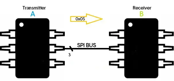
Yet, device B is printing out some random garbage!
The question is, who is the criminal to suspect? is it A? or B? or even the hardware bus on-board?
That’s why it’s kind of a tricky business to debug serial bus communications!
You just can’t decide which firmware has to be fixed. Arbitrarily suspicion & random modifications to either of firmware at A or B can make it more difficult and time-consuming. What I prefer, is to use one of the following methods
- An oscilloscope or Logic Analyzer (inspection)
- Standard virtual serial protocols debugger
I assume that everybody should be familiar with capturing signals on a generic CRO or a Logic analyzer. What I’d really like to point out to are the Virtual Serial Debugger Tools. Just a standard SPI receiver/transmitter which you can graphically configure using a GUI. Using it will make your life much easier, but why?
Well, if you’ve got a standard receiver that is guaranteed to correctly receive each and every data frame, Then you can tell if your SPI transmitter (device A) is malfunctioning or not!
Conversely, if you’ve got a standard transmitter that’s is guaranteed to generate and sens specific data frames at a specific baud rate flawlessly, Then you can tell if your SPI receiver (Device B) is malfunctioning or not!
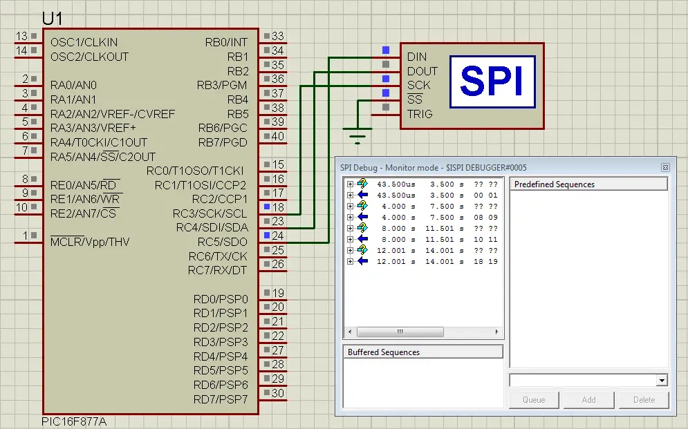
It’s available in proteus ISIS simulator and can be easily configured/connected as you’ve seen in the figure above. Use your own tools and what you personally prefer for debugging. Always be sure that you’re consistently stepping forward toward solving the problem or finding out who is the hiding criminal. And determine where and which changes have to be made!
7
Software SPI (Emulation)
The software can emulate an SPI transmitter/receiver module using only some code and consuming a considerable amount of resources specifically CPU’s time and/or a hardware timer. It can extend your available on-chip SPIs or compensate for the lack of a hardware SPI at all and to some extents. There is always fundamental limitations and drawbacks for what software can emulate.
All in all, if you’re in a situation where you need an additional SPI interface, you can emulate it using the software. Just in case your demand for an SPI is moderately low. But if your application needs extensive SPI communication with crazy high-speed data rates, then you should look for a native hardware solution. As overloading your CPU with unnecessarily expensive (in time) software will be a totally inefficient way to go.
8
SPI Related Definitions (Quick Review)
SCLK
The Serial Clock. It’s generated by the master which controls it’s frequency as well. The rate of SCK determines the data transfer rate. As each cycle, a single bit is transmitted/received.
MISO
The Master-In->Slave-Out.
MOSI
The Master-Out->Slave-In.
SS – SE
The Slave Select Line (Slave Enable). As long as it’s held High (Logic 1), No data can be received by the slave. The SPI Master controls the SS line/s in order to select which slave should receive the data. This line is usually an active low which required a low signal (Logic 0) to enable SPI data reception at the slave end.
CPOL – CKP
Clock Polarity. This term defines the IDLE state of the serial clock (SCK) whether it’s High or Low.
CPHA
Clock Phase. This term defines on which edge of the serial clock (SCK) the data will be transmitted whether it’s the leading edge or the trailing one.
Bit Sampling
When the input data is sampled (latched). It can be configured to sample the input at the end of the output data time or in the middle of it.
Write Collision
Any write to the SSPBUF register during transmission/reception of data will be ignored and the write collision detect bit (WCOL) will be set. User software must clear the WCOL bit so that it can be determined if the following write(s) to the SSPBUF register completed successfully.
Dummy Data
During each SPI clock cycle, full-duplex data transmission occurs. The master sends a bit on the MOSI line and the slave reads it, while the slave sends a bit on the MISO line and the master reads it. This sequence is maintained even when only one-directional data transfer is intended. Which means in order to receive any data you have to actually send something! in this case, we call it “Dummy Data” or “Junk”!
if you find this a useful resouece. Then, why not share it with your network ?!
You can also Support DeepBlue on patreon, paypal. Every single contribution helps alot. Cheers ^^
| Previous Tutorial | Tutorial 21 | Next Tutorial | |||||
Great Job!
When you will put the next tutorial?
This is the most comprehensive explanation that can be found. Great great work!!!
Thanks so much, my friend ^^
I’m so glad to hear this!
Hi.
I am an electronic student, at the moment we are learning about PIC Microcontroller and the SPI protocol.
So I trying to make this project in Proteus 8.
In the Master file I get this message:
Error at file ../main.c line 20 column 19: (141) can’t open include file “config.h”: No such file or directory
So It look like the header file config.h is missing.
Do you have any idea to solve this problem.
Hmmm. Try creating a new project with a new header configurations file. Then move your system to it, that may solve your issue
Hi am trying to write a code Pic16f72 with I2C(ds1307) using proteus can help me to write code. This is my wts app no 7204268734.
Check out this tutorial. It’s a gigantic guide on I2C with code examples for PIC16F parts
I hope it helps ^^
https://deepbluembedded.com/i2c-communication-protocol-tutorial-pic/
whats your email ? i got a project for you. my email is fomod2020@gmail.com
That was very informative tutorial. I want to ask what while(!BF); means.I could not find anything on internet about this.
Very very good and the most comprehensive Tutorials I have ever seen. All tutorials are great and crystal clear. Thanks a lot Sir Khaled Magdy.
Very good tutorial … what tools did you use to develop the simulations please.
I’m looking forward to reviewing your material. I noticed in the table under “Here is a brief comparison between serial communication and parallel communication protocols.” you have the ‘relative speed’ reversed.
Parallel is much faster than serial. That’s a key trade off. Speed vs. distance vs. #pins needed.
Greetings Brianv. Yes, I do agree that it seems counter-intuitive at the beginning. But the research i did back then confirmed such a thing. You can do a little bit of research for the parallel vs serial com max data transfer rate. I’ll be looking forward to seeing what you’d find.
Okay, let’s frame the issue properly. If we’re talking about leaving the motherboard (e.g. at the other end of a cable/wire/transmission line, then serial can indeed be faster for specific reasons:
Minimal crosstalk, need to ensure all parallel databits arrive at the same time, etc.
Nice write-up here: https://www.howtogeek.com/171947/why-is-serial-data-transmission-faster-than-parallel-data-transmission/.
After all, ethernet is serial, SATA is serial.
Thanks Brian! and I totally agree with that. And actually that’s what i’ve wrote in the article.
That uint8_t thing can you help me understand what that is please
Another way to declare an unsigned char ( 1 byte ) type of variable.
thanks, can you send any data type over the connection.
Yes, sure. We can send any data type however, multi-byte data types have to be handled in software by the programmer. In order to reconstruct the data at the receiving end.
May i know the name of the compiler, you written in this spi master slave code..
It’s XC8 Compiler from Microchip
Great tutorials , I feel I am learning a lot !! Just a quick question .. in the SPI _Read() function I can see BF=0; which I don’t fully understand ..I reckon that is bit 0 from the SSPSTAT register and that it is Read only and is set to 0 automatically by hardware as soon as SSPBUF is read . Am I missing something ? it is something I have also seen in the I2c tutorial. Thanks again for your great tutorials ..!!
Hi Juan!
Thanks for your note. As far as I can remember it was required in an MCU part that I used in the past which made me extra stressful over clearing that bit.
But as you’ve said in the datasheet it’s read only and automatically handled by hardware. This line of code is redundant ofcourse!
The 5th line of the SPI Master Full Code Listing should be SSPM1=1; for setting SCK Rate to Fosc/64.
The current code SSPM1=0; sets the SCK to Fosc/4.
Is there an update to this for newer PIC devices such as the PIC18F57Q43?
Is Khaled Magdy still available for tutorials?
Hi, thanks for checking up on me!
I’ve shifted away from Microchip PIC tutorials so many years ago and leaned more towards STM32 ARM-based MCUs to match the industry needs.
I’ve worked on many projects and consultations involving dsPIC devices and many other Microchip MCUs, but not as much 8-Bits target MCUs. They sure do exist in so many domains but not that I counter on a regular basis.