| Previous Tutorial | Tutorial 27 | Next Tutorial | |||||
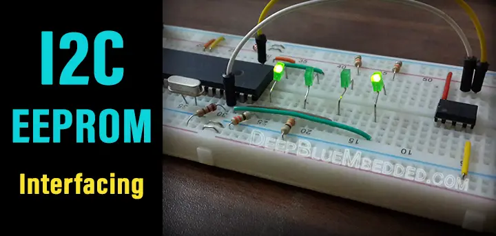
| Serial I2C EEPROM Interfacing With PIC MCUs | |||||||
| Intermediate Level ★★☆☆☆ | |||||||
In this tutorial, we’ll discuss the internal structure of serial I2C EEPROMs, how they work, and how to interface serial I2C EEPROM with PIC microcontrollers. And build a simple driver code example and practically test it in a quick LAB before concluding this tutorial. So, let’s get right into it!
[toc]
Components Needed For This Tutorial
| Qty. | Component Name | Buy On Amazon.com |
| 1 | PIC16F877A or PIC18F2550 or any other | Add |
| 1 | BreadBoard | Add |
| 8 | LED | Add Add |
| 1 | Resistors Kit | Add Add |
| 1 | Capacitors Kit | Add Add |
| 1 | Jumper Wires Pack | Add Add |
| 1 | LM7805 Voltage Regulator (5v) | Add |
| 1 | Crystal Oscillator | Add |
| 1 | PICkit2 or 3 Programmer | Add |
| 1 | 9v Battery or DC Power Supply | Add Add Add |
Debugging Tools:
- Digital Storage Oscilloscope (DSO): Siglent SDS1104 (on Amazon.com)
- Logic Analyzer (on Amazon.com)
I2C EEPROM 24C64
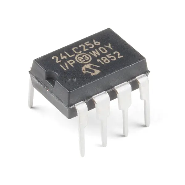
The 24C64 provides 65,536 bits (8kB) of serial electrically erasable and programmable read-only memory (EEPROM) organized as 8192 words of 8 bits each. The device’s cascadable feature allows up to 8 devices to share a common 2-wire (I2C) bus. The device is optimized for use in many industrial and commercial applications where low power and low voltage operation are essential.
Pinout & Functions
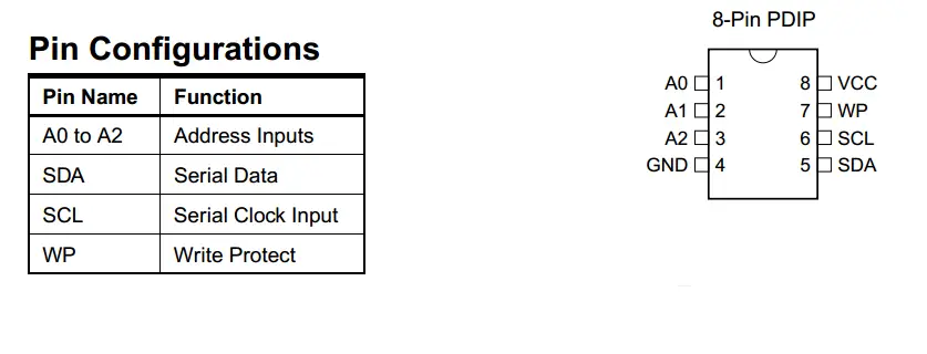
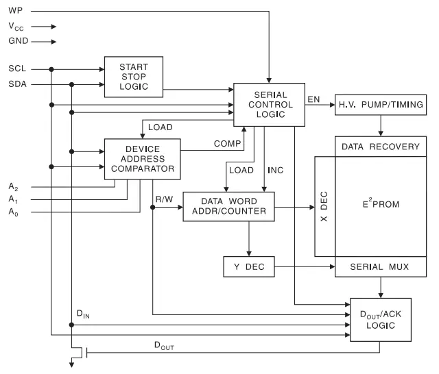
SERIAL CLOCK (SCL): The SCL input is used to positive edge clock data into each EEPROM device and negative edge clock data out of each device.
SERIAL DATA (SDA): The SDA pin is bidirectional for serial data transfer. This pin is open-drain driven and may be wire-ORed with any number of other open-drain or open-collector devices.
DEVICE/PAGE ADDRESSES (A2, A1, A0): The A2, A1, and A0 pins are device address inputs that are hard-wired or left not connected for hardware compatibility with AT24C16. When the pins are hardwired, as many as eight 32K/64K devices may be addressed on a single bus system (device addressing is discussed in detail under the Device Addressing section). When the pins are not hardwired, the default A2, A1, and A0 are zero.
WRITE PROTECT (WP): The write protect input, when tied to GND, allows normal write operations. When WP is tied high to VCC, all write operations to the upper quadrant (8/16K bits) of memory are inhibited. If left unconnected, WP is internally pulled down to GND.
Features
• Low-Voltage and Standard-Voltage Operation
– 5.0 (VCC = 4.5V to 5.5V)
– 2.7 (VCC = 2.7V to 5.5V)
– 2.5 (VCC = 2.5V to 5.5V)
– 1.8 (VCC = 1.8V to 5.5V)
• Low-Power Devices (ISB = 2 µA @ 5.5V) Available
• Internally Organized 8192 x 8
• 2-Wire (I2C) Serial Interface
• Schmitt Trigger, Filtered Inputs for Noise Suppression
• Bidirectional Data Transfer Protocol
• 100 kHz (1.8V, 2.5V, 2.7V) and 400 kHz (5V) Compatibility
• Write Protect Pin for Hardware Data Protection
• 32-Byte Page Write Mode (Partial Page Writes Allowed)
• Self-Timed Write Cycle (10 ms max)
• High Reliability
– Endurance: 1 Million Write Cycles
– Data Retention: 100 Years
– ESD Protection: >3,000V
Block Diagram
Reading & Writing To I2C EEPROM
The 64K EEPROM requires an 8-bit device address word following a start condition to enable the chip for a read or write operation. The device address word consists of a mandatory one, zero sequence (1010) for the first four most significant bits as shown. This is common to all 2-wire EEPROM devices.
The 64K uses the three device address bits A2, A1, A0 to allow as many as eight devices on the same bus. These bits must compare to their corresponding hardwired input pins. The A2, A1, and A0 pins use an internal proprietary circuit that biases them to a logic low condition if the pins are allowed to float.
The eighth bit of the device address is the read/write operation select bit. A read operation is initiated if this bit is high and a write operation is initiated if this bit is low. Upon a compare of the device address, the EEPROM will output a zero. If a compare is not made, the device will return to standby state.
Write Operations
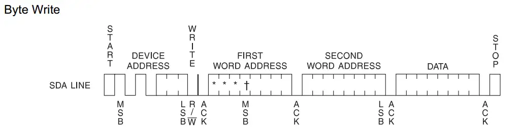
Single-Byte Write
A write operation requires two 8-bit data word addresses following the device address word and acknowledgment. Upon receipt of this address, the EEPROM will again respond with a zero and then clock in the first 8-bit data word. Following receipt of the 8-bit data word, the EEPROM will output a zero and the addressing device, such as a microcontroller, must terminate the write sequence with a stop condition.
At this time the EEPROM enters an internally-timed write cycle, tWR, to the nonvolatile memory. All inputs are disabled during this write cycle and the EEPROM will not respond until the write is complete.
Page Write
The 64K EEPROM is capable of 32- byte page writes. A page write is initiated the same way as a byte write, but the microcontroller does not send a stop condition after the first data word is clocked in. Instead, after the EEPROM acknowledges receipt of the first data word, the microcontroller can transmit up to 31 more data words. The EEPROM will respond with a zero after each data word received. The microcontroller must terminate the page write sequence with a stop condition.
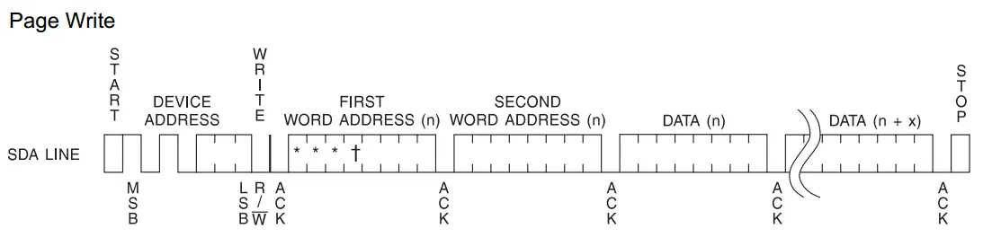
The data word address lower 5 bits are internally incremented following the receipt of each data word. The higher data word address bits are not incremented, retaining the memory page row location. When the word address, internally generated, reaches the page boundary, the following byte is placed at the beginning of the same page. If more than 32 data words are transmitted to the EEPROM, the data word address will “roll-over” and previous data will be overwritten.
Read Operations
Read operations are initiated the same way as write operations with the exception that the read/write select bit in the device address word is set to one. There are three read operations: current address read, random address read and sequential read.
Current Address Read
The internal data word address counter maintains the last address accessed during the last read or write operation, incremented by one. This address stays valid between operations as long as the chip power is maintained. The address “roll-over” during reading is from the last byte of the last memory page to the first byte of the first page. The address “roll-over” during write is from the last byte of the current page to the first byte of the same page.
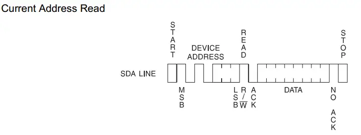
Once the device address with the read/write select bit set to one is clocked in and acknowledged by the EEPROM, the current address data word is serially clocked out. The microcontroller does not respond with an input zero but does generate a following stop condition.
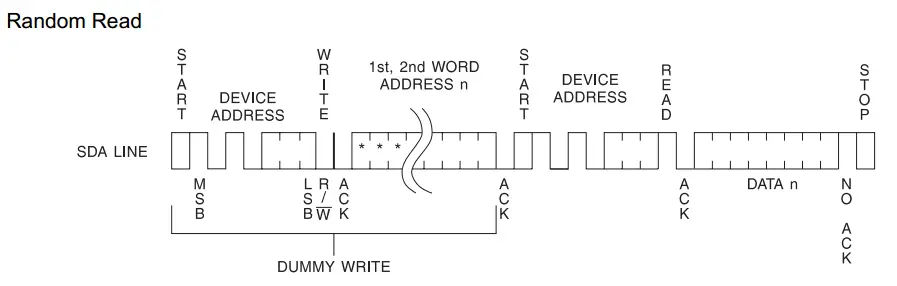
Random Address Read
A random read requires a “dummy” byte write sequence to load in the data word address. Once the device address word and data word address are clocked in and acknowledged by the EEPROM, the microcontroller must generate another start condition. The microcontroller now initiates a current address read by sending a device address with the read/write select bit high. The EEPROM acknowledges the device address and serially clocks out the data word. The microcontroller does not respond with a zero but does generate a following stop condition.
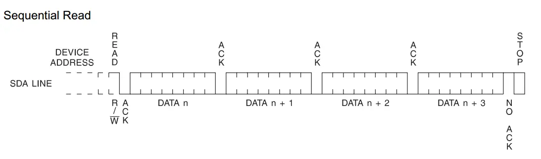
Sequential Read
Sequential reads are initiated by either a current address read or a random address read. After the microcontroller receives a data word, it responds with an acknowledge. As long as the EEPROM receives an acknowledge, it will continue to increment the data word address and serially clock out sequential data words. When the memory address limit is reached, the data word address will “roll-over” and the sequential read will continue. The sequential read operation is terminated when the microcontroller does not respond with a zero but does generate a following stop condition.
Implementing I2C EEPROM Driver
We’ll use the I2C device driver which we’ve implemented in the previous I2C Tutorial. And here is the header for the functions’ definitions in the I2C driver file.
|
1 2 3 4 5 6 7 8 9 10 |
//---[ I2C Routines ]--- void I2C_Master_Init(const unsigned long baud); void I2C_Master_Wait(); void I2C_Master_Start(); void I2C_Master_RepeatedStart(); void I2C_Master_Stop(); void I2C_ACK(); void I2C_NACK(); unsigned char I2C_Master_Write(unsigned char); unsigned char I2C_Read_Byte(void); |
We’ll Now Start Developing The Functions Below!
|
1 2 3 4 5 |
//---[ EEPROM Routines ]--- void EEPROM_Write(unsigned int add, unsigned char data); void EEPROM_Write_Page(unsigned int add, unsigned char* data, unsigned char len); unsigned char EEPROM_Read(unsigned int add); void EEPROM_Read_Page(unsigned int add, unsigned char* data, unsigned int len); |
EEPROM Write Operations
Single-Byte Write
|
1 2 3 4 5 6 7 8 9 10 11 12 13 14 |
// EEPROM Write Byte void EEPROM_Write(unsigned int add, unsigned char data) { I2C_Master_Start(); // Wait Until EEPROM Is IDLE while(I2C_Master_Write(EEPROM_Address_W)) I2C_Master_RepeatedStart(); I2C_Master_Write(add>>8); I2C_Master_Write((unsigned char)add); I2C_Master_Write(data); I2C_Master_Stop(); } |
Page Write
|
1 2 3 4 5 6 7 8 9 10 11 12 13 14 15 16 |
// EEPROM Write Page void EEPROM_Write_Page(unsigned int add, unsigned char* data, unsigned char len) { I2C_Master_Start(); // Wait Until EEPROM Is IDLE while(I2C_Master_Write(EEPROM_Address_W)) I2C_Master_RepeatedStart(); I2C_Master_Write(add>>8); I2C_Master_Write((unsigned char)add); for(unsigned int i=0; i<len; i++) I2C_Master_Write(data[i]); I2C_Master_Stop(); } |
EEPROM Read Operations
Random Byte Read
|
1 2 3 4 5 6 7 8 9 10 11 12 13 14 15 16 17 18 19 20 21 |
//---[ Byte Read ]--- unsigned char EEPROM_Read(unsigned int add) { unsigned char Data; I2C_Master_Start(); // Wait Until EEPROM Is IDLE while(I2C_Master_Write(EEPROM_Address_W)) I2C_Master_RepeatedStart(); I2C_Master_Write(add>>8); I2C_Master_Write((unsigned char)add); I2C_Master_RepeatedStart(); I2C_Master_Write(EEPROM_Address_R); Data = I2C_Read_Byte(); I2C_NACK(); I2C_Master_Stop(); return Data; } |
Sequential (Page) Read
|
1 2 3 4 5 6 7 8 9 10 11 12 13 14 15 16 17 18 19 20 |
//---[ Sequential Read ]--- void EEPROM_Read_Page(unsigned int add, unsigned char* data, unsigned int len) { I2C_Master_Start(); // Wait Until EEPROM Is IDLE while(I2C_Master_Write(EEPROM_Address_W)) I2C_Master_RepeatedStart(); I2C_Master_Write(add>>8); I2C_Master_Write((unsigned char)add); I2C_Master_RepeatedStart(); I2C_Master_Write(EEPROM_Address_R); for(unsigned int i=0; i<len; i++) { data[i] = I2C_Read_Byte(); I2C_ACK(); } I2C_Master_Stop(); } |
EEPROM Driver Complete Code Files
I2C_EEPROM.h
|
1 2 3 4 5 6 7 8 9 10 11 12 13 14 15 16 17 18 |
//-----------[ Functions' Prototypes ]-------------- //---[ I2C Routines ]--- void I2C_Master_Init(const unsigned long baud); void I2C_Master_Wait(); void I2C_Master_Start(); void I2C_Master_RepeatedStart(); void I2C_Master_Stop(); void I2C_ACK(); void I2C_NACK(); unsigned char I2C_Master_Write(unsigned char); unsigned char I2C_Read_Byte(void); //---[ EEPROM Routines ]--- void EEPROM_Write(unsigned int add, unsigned char data); void EEPROM_Write_Page(unsigned int add, unsigned char* data, unsigned char len); unsigned char EEPROM_Read(unsigned int add); void EEPROM_Read_Page(unsigned int add, unsigned char* data, unsigned int len); |
I2C_EEPROM.c
|
1 2 3 4 5 6 7 8 9 10 11 12 13 14 15 16 17 18 19 20 21 22 23 24 25 26 27 28 29 30 31 32 33 34 35 36 37 38 39 40 41 42 43 44 45 46 47 48 49 50 51 52 53 54 55 56 57 58 59 60 61 62 63 64 65 66 67 68 69 70 71 72 73 74 75 76 77 78 79 80 81 82 83 84 85 86 87 88 89 90 91 92 93 94 95 96 97 98 99 100 101 102 103 104 105 106 107 108 109 110 111 112 113 114 115 116 117 118 119 120 121 122 123 124 125 126 127 128 129 130 131 132 133 134 135 136 137 138 139 140 141 142 |
#include <xc.h> #include "I2C_EEPROM.h" #define _XTAL_FREQ 16000000 #define EEPROM_Address_R 0xA1 #define EEPROM_Address_W 0xA0 //---------------[ I2C Routines ]------------------- //-------------------------------------------------- void I2C_Master_Init(const unsigned long baud) { SSPCON = 0b00101000; SSPCON2 = 0; SSPADD = (_XTAL_FREQ/(4*baud))-1; SSPSTAT = 0; TRISC3 = 1; TRISC4 = 1; } void I2C_Master_Wait() { while ((SSPSTAT & 0x04) || (SSPCON2 & 0x1F)); } void I2C_Master_Start() { I2C_Master_Wait(); SEN = 1; } void I2C_Master_RepeatedStart() { I2C_Master_Wait(); RSEN = 1; } void I2C_Master_Stop() { I2C_Master_Wait(); PEN = 1; } unsigned char I2C_Master_Write(unsigned char data) { I2C_Master_Wait(); SSPBUF = data; while(!SSPIF); // Wait Until Completion SSPIF = 0; return ACKSTAT; } unsigned char I2C_Read_Byte(void) { //---[ Receive & Return A Byte ]--- I2C_Master_Wait(); RCEN = 1; // Enable & Start Reception while(!SSPIF); // Wait Until Completion SSPIF = 0; // Clear The Interrupt Flag Bit I2C_Master_Wait(); return SSPBUF; // Return The Received Byte } void I2C_ACK(void) { ACKDT = 0; // 0 -> ACK I2C_Master_Wait(); ACKEN = 1; // Send ACK } void I2C_NACK(void) { ACKDT = 1; // 1 -> NACK I2C_Master_Wait(); ACKEN = 1; // Send NACK } //====================================================== //---------------[ I2C EEPROM Routines ]---------------- //------------------------------------------------------ //-----[ Write Operations ]----- // EEPROM Write Byte void EEPROM_Write(unsigned int add, unsigned char data) { I2C_Master_Start(); // Wait Until EEPROM Is IDLE while(I2C_Master_Write(EEPROM_Address_W)) I2C_Master_RepeatedStart(); I2C_Master_Write(add>>8); I2C_Master_Write((unsigned char)add); I2C_Master_Write(data); I2C_Master_Stop(); } // EEPROM Write Page void EEPROM_Write_Page(unsigned int add, unsigned char* data, unsigned char len) { I2C_Master_Start(); // Wait Until EEPROM Is IDLE while(I2C_Master_Write(EEPROM_Address_W)) I2C_Master_RepeatedStart(); I2C_Master_Write(add>>8); I2C_Master_Write((unsigned char)add); for(unsigned int i=0; i<len; i++) I2C_Master_Write(data[i]); I2C_Master_Stop(); } //----------------------------- //-----[ Read Operations ]----- //---[ Byte Read ]--- unsigned char EEPROM_Read(unsigned int add) { unsigned char Data; I2C_Master_Start(); // Wait Until EEPROM Is IDLE while(I2C_Master_Write(EEPROM_Address_W)) I2C_Master_RepeatedStart(); I2C_Master_Write(add>>8); I2C_Master_Write((unsigned char)add); I2C_Master_RepeatedStart(); I2C_Master_Write(EEPROM_Address_R); Data = I2C_Read_Byte(); I2C_NACK(); I2C_Master_Stop(); return Data; } //---[ Sequential Read ]--- void EEPROM_Read_Page(unsigned int add, unsigned char* data, unsigned int len) { I2C_Master_Start(); // Wait Until EEPROM Is IDLE while(I2C_Master_Write(EEPROM_Address_W)) I2C_Master_RepeatedStart(); I2C_Master_Write(add>>8); I2C_Master_Write((unsigned char)add); I2C_Master_RepeatedStart(); I2C_Master_Write(EEPROM_Address_R); for(unsigned int i=0; i<len; i++) { data[i] = I2C_Read_Byte(); I2C_ACK(); } I2C_Master_Stop(); } |
I2C EEPROM Test – LAB1
| Lab Name | I2C Serial EEPROM Interfacing (Single-Byte Write & Read) |
| Lab Number | 32 |
| Lab Level | Intermediate |
| Lab Objectives | Learn how to use I2C Communication works. And interface the I2C Serial EEPROM 24C64 Memory. Do some data transactions (single-byte transfers) and (bulk data transfers). |
1. Coding
Open the MPLAB IDE and create a new project and name it “I2C_EEPROM”. If you have some issues doing so, you can always refer to the previous tutorial using the link below.

Set the configuration bits to match the generic setting which we’ve stated earlier. And if you also find troubles creating this file, you can always refer to the previous tutorial using the link below.

Now, open the main.c file and let’s start developing the firmware for our project.
Start your project by including the I2C_EEPROM.h driver library which we’ve developed earlier in this tutorial. Then do some random byte write followed by single read operations and display the bytes on PORTD to check the validity.
The Full Code Listing For This Lab
|
1 2 3 4 5 6 7 8 9 10 11 12 13 14 15 16 17 18 19 20 21 22 23 24 25 26 27 28 29 30 31 32 33 34 35 36 37 |
/* * File: main.c * Project: I2C EEPROM Interfacing * Author: Khaled Magdy * Visit @ https://deepbluembedded.com */ #include <xc.h> #include "config.h" #include "I2C_EEPROM.h" #define _XTAL_FREQ 16000000 void main(void) { I2C_Master_Init(100000); unsigned int Address = 0x0020; // Some Random Address unsigned char Data = 0x04; // Some Random Data To Write EEPROM_Write(Address++, Data++); // Write 0x04 @ 0x0020 EEPROM_Write(Address++, Data++); // Write 0x05 @ 0x0021 EEPROM_Write(Address, Data); // Write 0x06 @ 0x0022 __delay_ms(10); // Wait tWR=10ms For Write To Complete Address = 0x0020; // Point To First Byte Location TRISD = 0x00; PORTD = EEPROM_Read(Address++); // Should Read 0x04 __delay_ms(1000); PORTD = EEPROM_Read(Address++); // Should Read 0x05 __delay_ms(1000); PORTD = EEPROM_Read(Address); // Should Read 0x06 __delay_ms(1000); while(1) { // Stay IDLE .. DO Nothing! } return; } |
2. Simulation
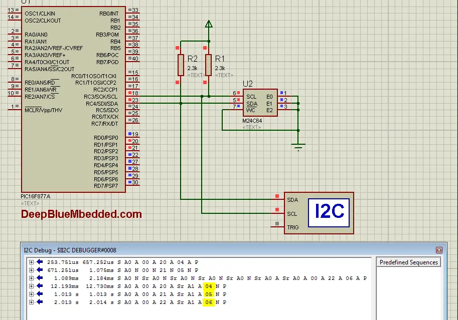
Here are the simulation results. As you can see, the MCU firstly attempts to write the following bytes (0x04, 0x05, 0x06) to the following addresses (0x0020, 0x0021, 0x0022). Then, it starts to read out these locations one by one and the data being read should be (0x04, 0x05, 0x06) in order. And that’s what is going on right here!
3. Prototyping
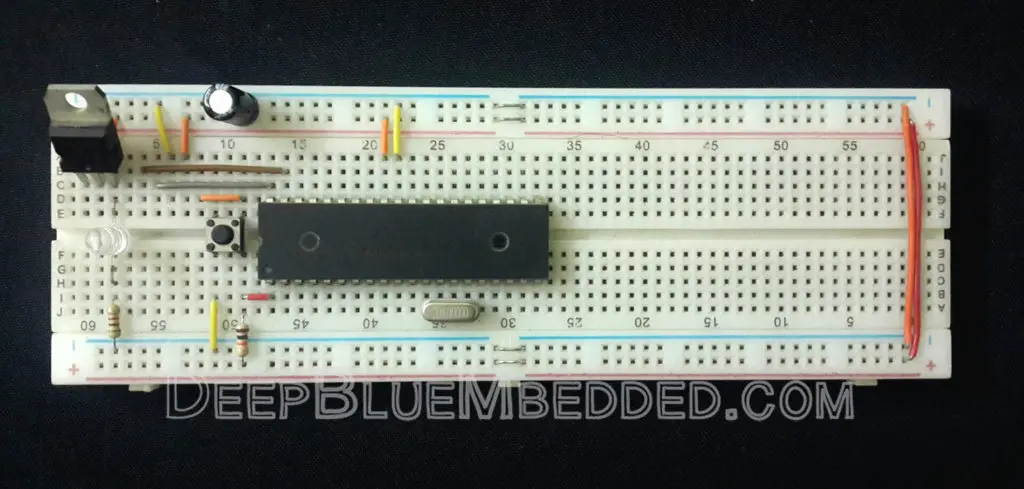
Down below is the real-life running test for this LAB on real boards. It’s very easy to hook everything up in this LAB. And it might be challenging to get it to work in case you MCU has different hardware implementation that needs a little bit of tweaking in code to get it to work well.
 |
Download I2C EEPROM LAB1 Project (Code+Simulation)
I2C EEPROM Test – LAB2
| Lab Name | I2C Serial EEPROM Interfacing (Page Write & Read) |
| Lab Number | 33 |
| Lab Level | Intermediate |
| Lab Objectives | Learn how to use I2C Communication works. And interface the I2C Serial EEPROM 24C64 Memory. Do some data transactions (single-byte transfers) and (bulk data transfers). |
1. Coding
Open the MPLAB IDE and create a new project and name it “I2C_EEPROM”. If you have some issues doing so, you can always refer to the previous tutorial using the link below.
Set the configuration bits to match the generic setting which we’ve stated earlier. And if you also find troubles creating this file, you can always refer to the previous tutorial using the link below.
Now, open the main.c file and let’s start developing the firmware for our project.
Start your project by including the I2C_EEPROM.h driver library which we’ve developed earlier in this tutorial. Then do some random page write followed by page read operation and display the bytes on PORTD to check the validity.
The Full Code Listing For This Lab
|
1 2 3 4 5 6 7 8 9 10 11 12 13 14 15 16 17 18 19 20 21 22 23 24 25 26 27 28 29 30 31 32 33 34 35 36 37 38 |
/* * File: main.c * Project: I2C EEPROM Interfacing * Author: Khaled Magdy * Visit @ https://deepbluembedded.com */ #include <xc.h> #include "config.h" #include "I2C_EEPROM.h" #define _XTAL_FREQ 16000000 void main(void) { I2C_Master_Init(100000); unsigned int Address = 0x0020; // Some Random Address // Some Random Data BufferTo Write unsigned char Buffer[5] = {0x05, 0x06, 0x07, 0x08, 0x09}; unsigned char ReadBuffer[5]; //---[ Write Page ]--- EEPROM_Write_Page(Address, Buffer, 5); __delay_ms(10); // Wait tWR=10ms For Write To Complete //---[ Read Page ]--- TRISD = 0x00; EEPROM_Read_Page(Address, ReadBuffer, 5); for(int i=0; i<5; i++) { PORTD = ReadBuffer[i]; __delay_ms(1000); } while(1) { } return; } |
2. Simulation
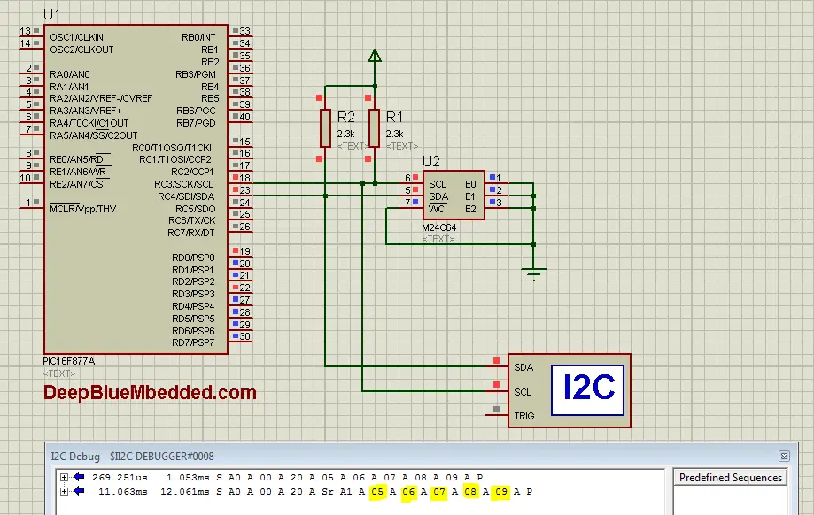
Here are the simulation results. As you can see, the microcontroller attempts to write a page of data (5 Bytes) @ address 0x0020 this page contains (0x05, 0x06, 0x07, 0x08, 0x09) in order. Then, a page read operation is performed and the ReadBuffer array is sent to PORTD byte by byte. And you can check the highlighted values which are exactly what we’d expect to come out of these memory locations.
3. Prototyping
Down below is the real-life running test for this LAB on real boards. It’s very easy to hook everything up in this LAB. And it might be challenging to get it to work in case you MCU has different hardware implementation that needs a little bit of tweaking in code to get it to work well.
|
Download I2C EEPROM LAB2 Project (Code+Simulation)
| Previous Tutorial | Tutorial 27 | Next Tutorial | |||||
Thanks!