Analog To Digital Converter | How ADC Works And Reading Analog Signals
| Previous Tutorial | Tutorial 22 | Next Tutorial | |||||
| Embedded Systems Tutorials With PIC MCUs | |||||||
| Intermediate Level ★★☆☆☆ | |||||||
In this tutorial, you’ll get a solid introduction to the analog signal conversion to the digital domain. And why it’s important to do so. And how does ADC work in order to achieve such a goal? And what are the fundamental limitations and challenges for practical ADC? We’ll also see different schemes for how to read an ADC with an 8-Bit Microcontroller from Microchip (PIC). By the end of this long tutorial, you’ll understand the fundamental foundations of ADC and you’ll also create the 2 projects below from scratch. And have your own device driver for ADC for any future project you wanna create. Stick with me it’s gonna be so long, hopefully, informative journey! And let’s get started!
[toc]
Required Components
| Qty. | Component Name | Buy On Amazon.com |
| 1 | PIC16F877A | Add |
| 1 | BreadBoard | Add |
| 1 | Potentiometer | Add Add |
| 1 | LED | Add Add |
| 1 | Microphone | Add Add |
| 1 | BC337 NPN BJT Transistor | Add Add |
| 1 | Resistors Kit (to build audio amp.) | Add Add |
| 1 | Capacitors Kit (to build audio amp.) | Add Add |
| 1 | USB-TTL (FTDI) Serial Converter | Add |
| 1 | Jumper Wires Pack | Add Add |
| 1 | LM7805 Voltage Regulator (5v) | Add |
| 1 | Crystal Oscillator | Add |
| 1 | PICkit2 or 3 Programmer | Add |
What is Analog To Digital Conversion?
It’s a process of capturing the analog electric signal (such as sound captured by a microphone) and converting it to a series of numeric “Digital” values to be stored/processed by a digital computer or DSP. The electronic device which is used for this conversion process has been known to be the A/D or ADC (Analog-To-Digital Converter).
There are many different types of A/D converters out there. And depending on how it works and how well it gets the job done, you pay more or less respectively per ADC unit.
And before any further investigation for ADC types and technical details of working principles, let us question about the usefulness of A/D conversion. Why do we need to use ADC in the first place?
Why We Need Analog To Digital Converters?
Our need to convert analog signals to digital data stems from the fact that our computers are digital ones. They just can’t handle the analog signal and therefore, there should be a device which converts the signal from analog to digital domain (ADC).
Most signals are analog in nature and the electronic sensors which we’re using for capturing these phenomena are also analog. For example, the temperature sensor converts temperature in °C to an analog voltage that’s proportional to the value of temperature. So do the microphone, pressure sensor, light sensor and so on.
Hence, we need a way to read analog voltage and convert it to digital values which we can program our computers to manipulate it mathematically in order to achieve real-time monitoring and/or control or whatever.
Image Credit to Ti.com
How ADC Works?
General Block Diagram For ADC
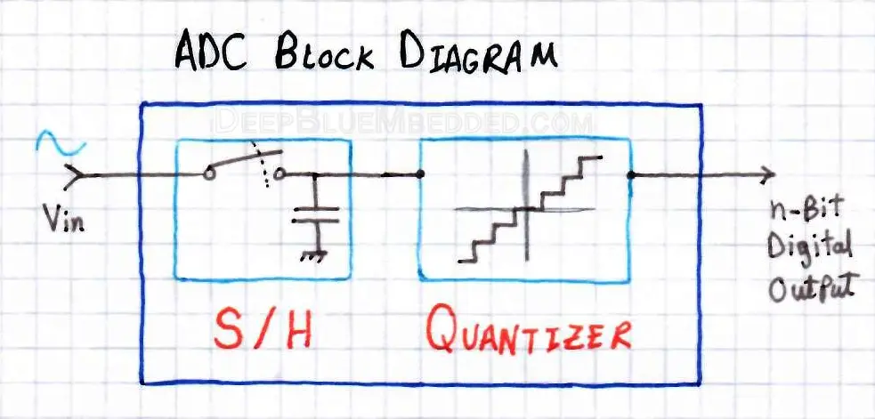
The basic structure of an ADC consists of an S/H circuit (Sample & Hold). Followed by a quantized which is actually the working horse for the analog to the digital conversion process. The type of ADC depends on how it’s performing the quantization process, it can be analog integration, digital counter, successive approximation, or even direct conversion as in Flash ADC types which we’ll discuss hereafter.
Finally, the digital output data is served to the CPU or gets directly stored in memory. The ADC can either be integrated within the MCU chip itself or a standalone IC that you can interface with Serial/Parallel ports of your microcontroller.
Analog Reference For ADC
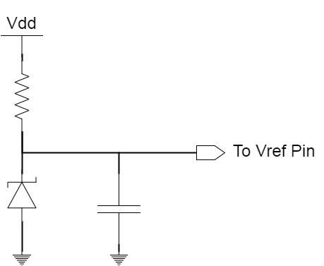
Analog To Digital Conversion process needs an extremely stable voltage reference Vref+ and Vref– representing the maximum allowable voltage swing for the input in order to be correctly converted to digital value with respect to the limits which are set by the analog reference Vref.
The easiest way to guarantee a stable Vref is to use a resistor and a capacitor to resist any sudden drop in voltage and protect your system. You can also use a Zener diode as well to guarantee a stable voltage reference which immunes your system against any sudden changes in power supply increase/drop. The concept is indicated in the diagram below.
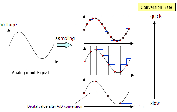
ADC Sampling
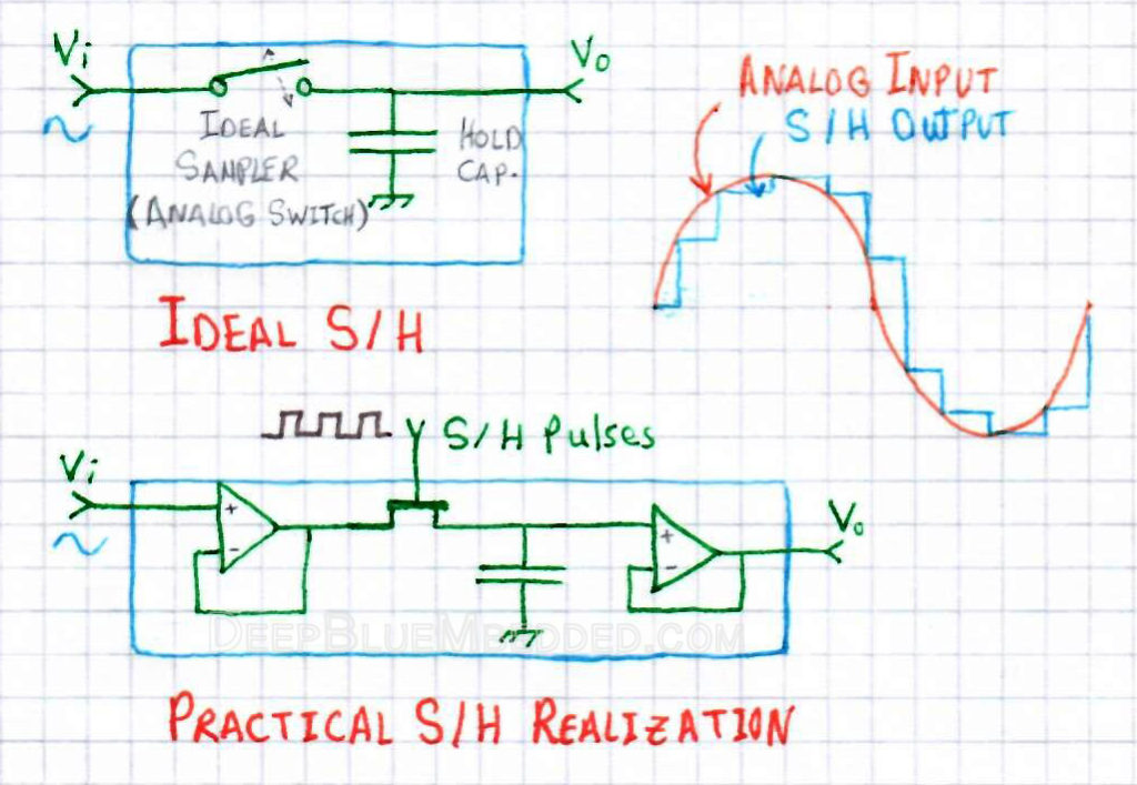
The Analog input signal which is a continuous function in time has to be held constant for a short period of time during which the ADC can convert the instantaneous value to its digital representation. This process is done by the Sample/Hold circuitry which is basically an Analog Switch + a Holding Capacitor. It can get more complicated in advanced converters but we’re assuming the very basic S/H circuitry.
Sampling Rate
The rate at which an ADC converts the continuous analog signal to digital data is called “Sampling Rate”. And if it takes Ts time to convert a single sample, then the sampling rate of this ADC is Fs = 1/Ts. Then the original analog signal can be reproduced from the discrete-time digital values by mathematical interpolation. The accuracy in this procedure is dictated by the combined effect of the sampling rate and quantization error.
Sampling Theorem
Theoretically, and to get the minimal information about the original analog signal, an ADC must sample and convert the analog signal with a frequency of Fs >= 2FMAX Which satisfies the Shannon-Nyquist sampling theorem.
Fs -> The Sampling Frequency of an ADC
FMAX -> The Maximum Frequency In The Analog Signal Being Converted
Violating this rule will lead to further problems and loss of significant information about the signal. It’s near to impossible to get an idea of what does the original signal look like before conversion. That’s why we practically pick an ADC with a sampling rate (Fs) of about 10 x FMAX To avoid operating near to the fundamental limitations of the sampling.
Over-Sampling
Analog signals are usually sampled at the minimum allowable frequency for economical reasons. However, if an analog signal is sampled at a much higher rate than the Nyquist limitation and then got filtered by a digital filter to limit its bandwidth, we’ll have many interesting results “Achievements in fact”. For example, a 20-bit ADC can be made to act as a 24-bit ADC with 256× oversampling.
The over-sampling technique is typically used in audio frequency ADCs where the required sampling rate (typically 44.1kHz) is very low compared to the clock speed of typical logic circuits (>1MHz). In this case, by using the extra bandwidth to distribute quantization error onto out of band frequencies, the accuracy of the ADC can be greatly increased at no additional cost.
ADC Resolution & Quantization
Resolution
The Resolution of an ADC indicates the number of discrete values it can produce over the range of analog values. The Resolution also determines the magnitude of the quantization error and therefore determines the maximum possible average signal-to-noise ratio (SNR) for a typical ADC.
The resolution Q depends on both the number of bits n generated by the quantizer and also the FSR (full-scale range) for the analog reference voltage line. Here is the formula to calculate the resolution of quantization Q which is basically a division for the FSR voltage by the number of levels 2n
![]()
Which means, an 8-Bit ADC with an analog reference Vref+of 5v has a resolution of
![]()
That’s why you can potentially increase the ADC conversion resolution by decreasing the analog voltage reference provided that you’re measuring small signals. Alternatively, you can amplify small signals like audio sound captured by a microphone which is typically in milli-volts range.
Quantization
The quantizer circuit is the working horse of an ADC. Its function is to convert the analog voltage captured by the S/H circuitry to the digital corresponding value. There are many schemes for creating a quantization circuit which also determines the type of an ADC. What you should really know in the meantime, that the quantization process whether it’s rounding-off or truncating intermediate analog signals which lie between two Q levels.
Quantization Error
The quantization error is due to the fact that analog signals will always lie between two distinct Q levels. Should we round-off or truncate? doing either will generate what we call “The Quantization Error”. And it can’t be avoided, However, we can improve the overall accuracy using different techniques.
The Signal To Quantization Noise Ratio (SQNR) is calculated using the following formula
![]()
There are many different schemes used by different types of ADCs for analog signal quantization. Hence, we have a variety of ADC types which we’ll be discussing hereafter. Most of which use analog comparators alongside a digital counter, analog integrator, or a D/A in order to achieve the Analog To Digital conversion.
Different Types of ADC
There are many types for Analog To Digital Converters depending on the way they work. Here I’ll list some of the most commonly used ones whether for standalone ADC ICs or being integrated within microcontrollers. You can definitely research for whichever seems interesting to you as this is not going to be a heavily detailed demonstration.
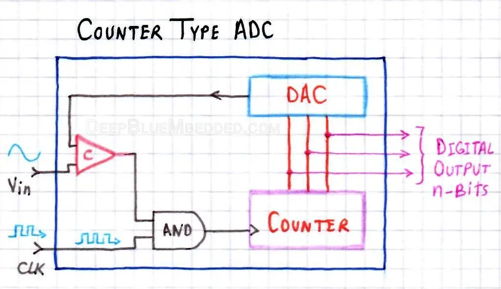
Counter Type ADC
This type of ADC utilizes a DAC (Digital To Analog Converter) in order to perform a quick sweep for the output voltage up to the point where the analog comparator confirms that the output voltage is nearly equal to the analog input signal being measured. Therefore, the counter stops sweeping and its current value is the direct digital representation for the input signal.
The block diagram down below indicates how a Counter Type ADC works
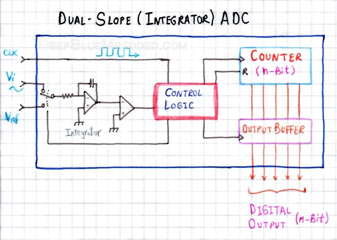
Integrating (Dual-Slope) ADC
An integrating ADC (dual-slope ADC) applies the analog input voltage to the input of an integrator and allows the voltage to ramp for a fixed time period (the run-up period). Then a known reference voltage of opposite polarity is applied to the integrator and is allowed to ramp until the integrator output returns to zero (the run-down period).
The input voltage is computed as a function of the reference voltage, the constant run-up time period, and the measured run-down time period. The run-down time measurement is usually made in units of the converter’s clock, so longer integration times allow for higher resolutions.
The block diagram indicating the functionality of Dual-Slope (Integrating) ADC is shown below.
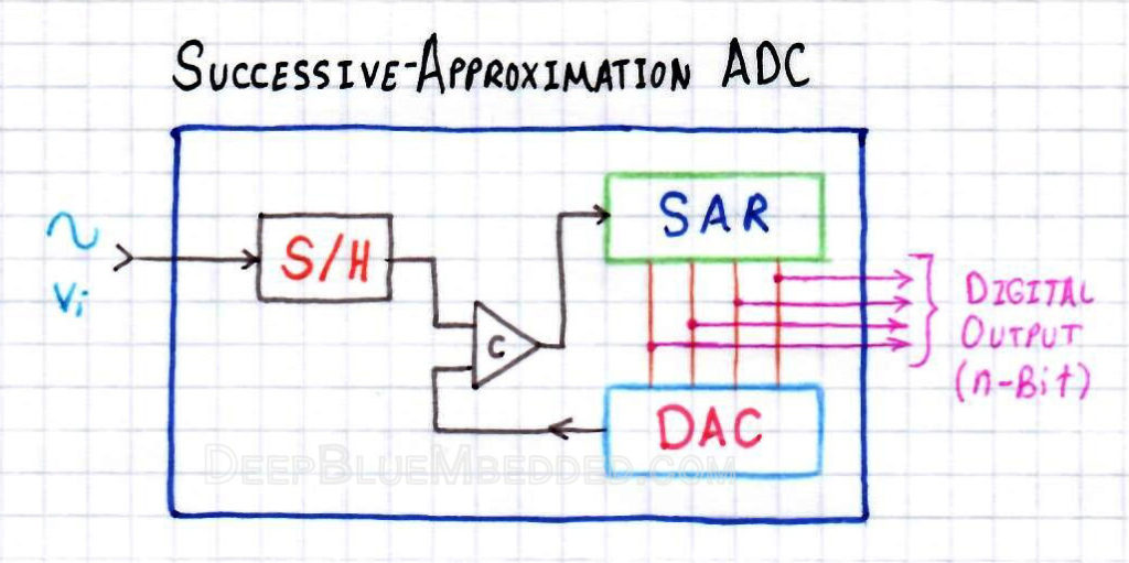
Successive Approximation
The Successive Approximation ADC uses a comparator to successively narrow a range that contains the analog input voltage. At each successive step, the converter compares the input voltage to the output of an internal DAC which might represent the midpoint of a selected voltage range. At each step in this process, the approximation is stored in the successive approximation register (SAR).
The block diagram indicating the functionality of Successive Approximation ADC is shown below.
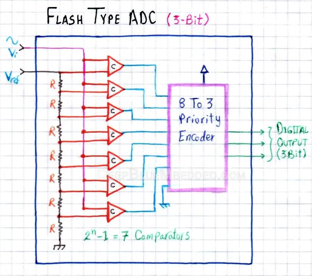
Flash Type ADC (Direct)
The Flash type ADC consists of (2n-1) parallel analog comparators. These comparators are sampling the analog input signal in parallel and driving the logic circuit which generates the digital code for each voltage level. It’s also called direct conversion as it’s the fastest type of ADC at all.
However, it’s limited in resolution. Typically 8-Bits are being used commonly, as increasing the resolution by a single 1 bit will require twice the number of comparators being used. And therefore, it’s extremely expensive and has a large size.
The block diagram indicating the functionality of Flash Type ADC (3-Bit) is shown below.
ADC Module in PIC Microcontroller
For the rest of this tutorial, we’ll discuss the ADC Module in PIC16F microcontrollers. How it works and how to configure and use it to read analog channels for our projects.
Hardware Description
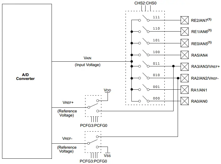
The Analog-to-Digital (A/D) Converter module has 5-Channels for the 28-pin devices and 8-Channels for the 40/44-pin devices. The conversion of an analog input signal results in a corresponding 10-Bit digital number.
The A/D module has high and low-voltage reference input that is software selectable to some combination of VDD, VSS, RA2 or RA3.
The A/D converter has a unique feature of being able to operate while the device is in Sleep mode. To operate in Sleep, the A/D clock must be derived from the A/D’s internal RC oscillator.
Block Diagram
Here is the block diagram for the A/D converter in out PIC16F877A microcontroller.
ADC Special Function Registers
The A/D module has four registers. These registers are
- A/D Result High Register (ADRESH)
- A/D Result Low Register (ADRESL)
- A/D Control Register 0 (ADCON0)
- A/D Control Register 1 (ADCON1)
The A/D conversion 10-Bit result is stored in (ADRESH+ADRESL) registers.
The operation of the ADC module is completely controlled by (ADCON0+ADCON1) registers.
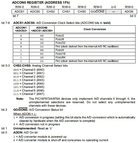
ADCON0 Register
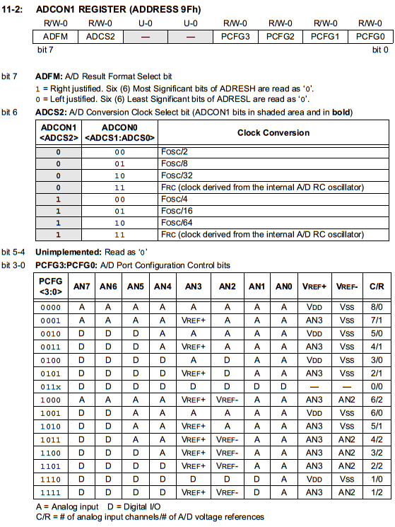
ADCON1
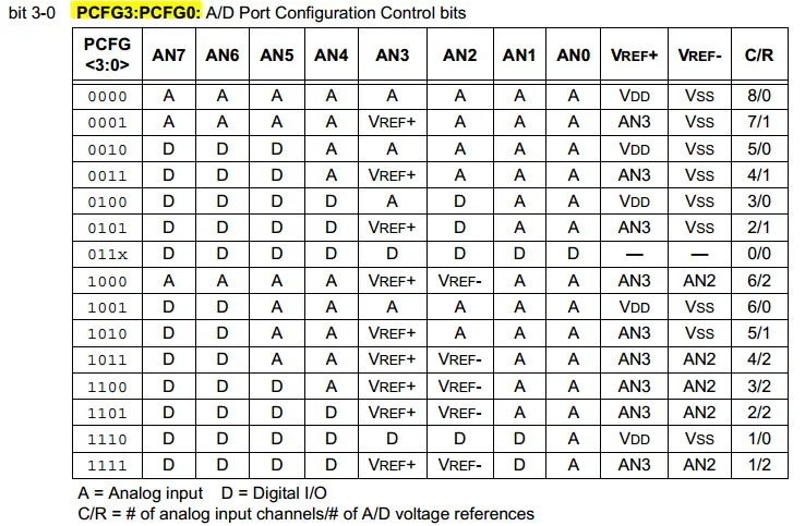
Analog Reference
The A/D module has high and low-voltage reference input that is software selectable to some combination of VDD, VSS, RA2 or RA3. You can select the voltage references in the same way as analog channel selection using the table above.
Let’s assume a Vref+ of VDD = 5v and Vref– of Vss = 0v for this tutorial. Which results in a full-scale range (FSR) of 5v. Therefore, the A/D conversion resolution will be
![]()
Channel Selection
In our microcontroller’s ADC module, there are 8 Analog Channels. These channels are multiplexed to a single 1 A/D converter, that’s why an analog switch exists in the block diagram. And you, the programmer, has to select the desired channel before an A/D conversion is initiated.
The ADCON1 and TRIS registers control the operation of the A/D port pins. The port pins that are desired as analog inputs must have their corresponding TRIS bits set (input). If the TRIS bit is cleared (output), the digital output level (VOH or VOL) will be converted. The A/D operation is independent of the state of the (CHS2:CHS0) bits and the TRIS bits.
A/D Aquisition Time
After the A/D module has been configured as desired, the analog signal of the selected channel must be acquired before the conversion is started. The analog input channels must have their corresponding TRIS bits selected as inputs. After this acquisition time has elapsed, the A/D conversion can start.
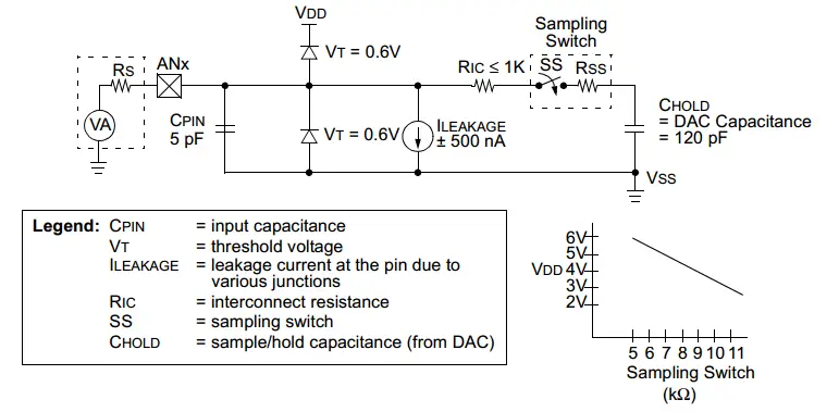
For the A/D converter to meet its specified accuracy, the charge holding capacitor (CHOLD) must be allowed to fully charge to the input channel voltage level.
The maximum recommended impedance for analog sources is 2.5 kΩ. As the impedance is decreased, the acquisition time may be decreased. After the analog input channel is selected (changed), this acquisition must be done before the conversion can be started.
To calculate the minimum acquisition time TACQ, you can use the equation below. This equation assumes that 1/2 LSB error is used (1024 steps for the A/D). The 1/2 LSB error is the maximum error allowed for the A/D to meet its specified resolution.
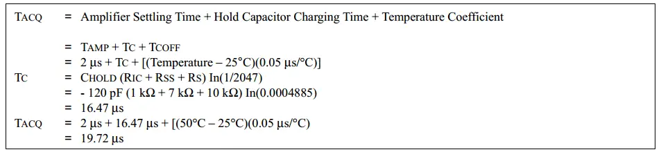
This equation is derived depending on the analog input model circuitry in the diagram below. And you can optimize your system for much lower acquisition time by a little bit more investigation in this model. Alternatively, you can shoot for a safe value instead.
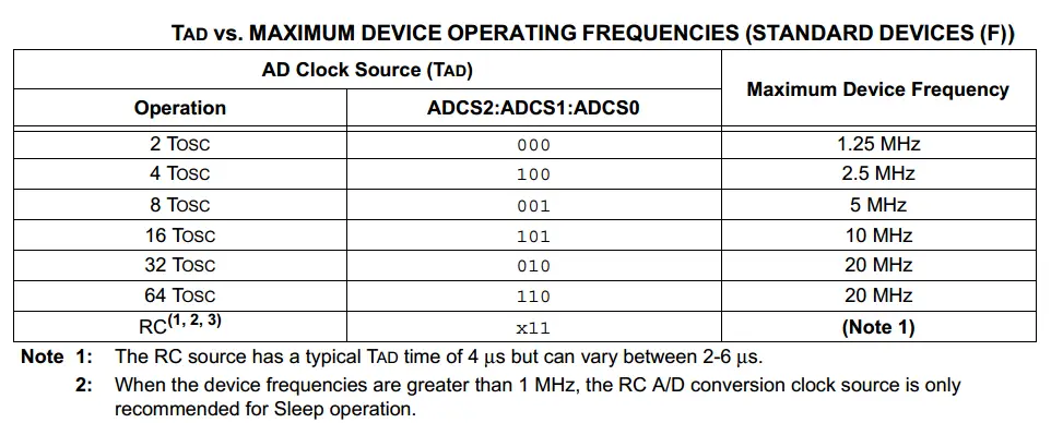
A/D Conversion Clock Selection
The A/D conversion time per bit is defined as TAD. The A/D conversion requires a minimum of 12 TAD per 10-bit conversion. The source of the A/D conversion clock is software selected. The seven possible options for TAD are:
- 2 TOSC
- 4 TOSC
- 8 TOSC
- 16 TOSC
- 32 TOSC
- 64 TOSC
- Internal A/D module RC oscillator (2-6 µs)
For correct A/D conversions, the A/D conversion clock (TAD) must be selected to ensure a minimum TAD time of 1.6 µs. The table below shows the resultant TAD times derived from the device operating frequencies and the A/D clock source selected.
Starting A/D Conversion
Setting the GO/DONE bit starts a new conversion for the selected channel. A new conversion should not start before the Aquisition Time TACQ has elapsed.
Clearing the GO/DONE bit during a conversion will abort the current conversion. The A/D Result register pair will NOT be updated with the partially completed A/D conversion sample. That is, the (ADRESH:ADRESL) registers will continue to contain the value of the last completed conversion (or the last value written to the ADRESH:ADRESL registers). After the A/D conversion is aborted, the next acquisition on the selected channel is automatically started. The GO/DONE bit can then be set to start the conversion.
The figure below indicates the A/D conversion cycles that it takes to convert an analog signal since setting the GO/DONE bit until the result is written to the ADRES registers. Also note that after the GO bit is set, the first time segment has a minimum of TCY and a maximum of TAD.
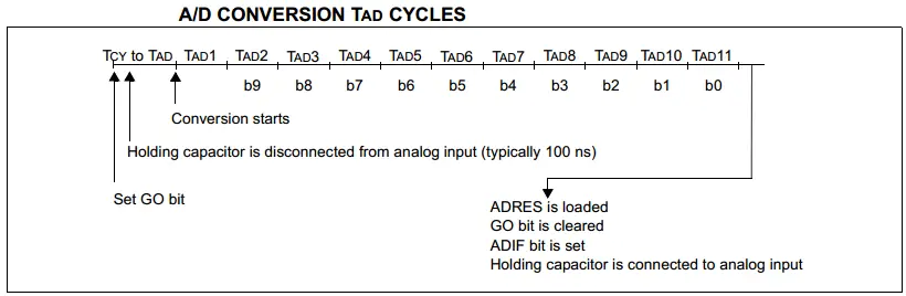
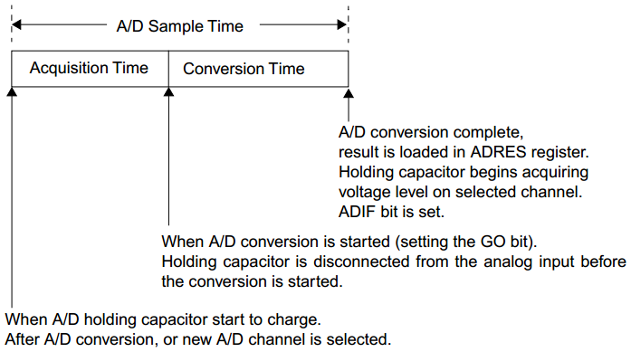
A/D Conversion Sequence Timing
The following diagram will show you the A/D conversion sequence and will also indicate the timing terminology. The acquisition time TACQ is the time that the A/D module’s holding capacitor is connected to the external voltage level.
Then there is the conversion time TC of 10 TAD, which is started when the GO bit is set. The sum of these two times is the sampling time TS. Hence, the sampling frequency FS = 1 / TS.
There is a minimum acquisition time to ensure that the holding capacitor is charged to a level that will give the desired accuracy for the A/D conversion.
A/D Conversion Result Registers
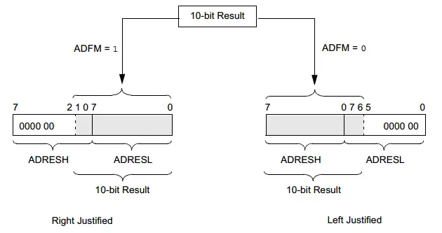
The (ADRESH:ADRESL) register pair is the location where the 10-bit A/D result is loaded at the completion of the A/D conversion. This register pair is 16 bits wide. The A/D module gives the flexibility to left or right justify the 10-bit result in the 16-bit result register.
The A/D Format Select bit (ADFM) controls this justification. The figure below shows the operation of the A/D result justification. Where the extra bits are loaded with ‘0’s.
Maximum Sampling Rate
Maximizing the sampling rate of your ADC is obviously a hard task to go for. However, in some situations, you’ll actually need to get as many samples as you can out of your ADC. So, here are a few things to consider.
Analog channel switching requires additional wait time “Aquisition Time TACQ“. So, if all that you need is a single channel, then you can save so much time as there is no need to switch between channels and unnecessarily waste so much time waiting for CHOLD to charge each time.
Another thing, you can sacrifice the accuracy of your ADC conversion reading for pushing the maximum sampling rate a little bit further.
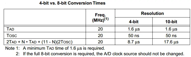
The A/D converter allows you to make the trade-off of conversion speed to resolution. Regardless of the resolution required, the acquisition time is the same. To speed up the conversion, the clock source of the A/D module may be switched so that the TAD time violates the minimum specified time (Shown previously, TADmin = 1.6µs).
Once the TAD time violates the minimum specified time, all the following A/D result bits are not valid. The clock sources may only be switched between the FOSC derived options (cannot be switched from/to RC). The equation to determine the time before the oscillator can be switched is as follows:
Conversion time TC = TAD + N • TAD + (11 – N)(2TOSC)
Where N = number of bits of resolution required
Since the TAD is based on the device oscillator, you must use a method (a timer, software loop, etc.) to determine when the A/D oscillator may be changed.
The following example in the table below shows a comparison of time required for a conversion with 4-bits of resolution, versus the 10-bit resolution conversion. The example is for devices operating at 20MHz (The A/D clock is programmed for 32TOSC) and assumes that immediately after 6TAD, the A/D clock is programmed for 2TOSC. The 2TOSC violates the minimum TAD time since the last 4 bits will not be converted to correct values. And that’s the trick for speeding it up!
Configuring ADC With PIC MCU
Steps To Configure The ADC Module
To do an A/D Conversion, Follow these steps:
1. Configure the A/D module
• Configure analog pins/voltage reference and digital I/O (ADCON1)
• Select A/D input channel (ADCON0)
• Select A/D conversion clock (ADCON0)
• Turn on A/D module (ADCON0)
2. Configure A/D interrupt (if desired):
• Clear ADIF bit
• Set ADIE bit
• Set PEIE bit
• Set GIE bit
3. Wait the required acquisition time.
4. Start conversion
• Set GO/DONE bit (ADCON0)
5. Wait for A/D conversion to complete by either:
• Polling for the GO/DONE bit to be cleared (interrupts disabled); OR
• Waiting for the A/D interrupt
6. Read A/D Result register pair (ADRESH:ADRESL), clear bit ADIF if required.
7. For the next conversion, go to step 1 or step 2 as required. The A/D conversion time per bit is defined as TAD.
Implementing Simple ADC Driver
Step1 Configure The ADC Module
All Analog Channels Are Activated, Vref+ = Vdd, Vref- = Vss
Our Fosc = 4MHz, so we’ll choose the ADC clock to be FOSC/8, so 8TOSC = 2μs. Which satisfies the condition of TAD must be larger than 1.6μs.
And finally, Turn ON the ADC module
|
1 |
ADCON0 = 0x41; // Turn ADC ON, Select AN0 Channel, ADC Clock = Fosc/8 |
Let’s set the A/D conversion result justification to be “Right-Justified”
Let’s select AN0 channel for example
|
1 2 |
ADCON1 = 0x80; // All 8 Channels Are Analog, Result is "Right-Justified" // ADC Clock = Fosc/8 |
Step2 Configure A/D interrupts (if desired)
|
1 2 3 4 |
ADIF = 0; // Clear ADC Interrupt Flag ADIE = 1; // ADC Interrupt Enable Bit PEIE = 1; // Peripherals Interrupt Enable Bit GIE = 1; // Global Interrupts Enable Bit |
Step3 Wait The Required Aquisition Time TACQ
|
1 |
__delay_us(30); // The Minimum Tacq = 20us, So That should be enough |
Step4 Start The A/D Conversion
|
1 |
GO_DONE = 1; // Start A/D Conversion |
Step5 Wait for A/D conversion to complete by either
1. Polling The GO/DONE Bit
|
1 2 |
while(ADCON0bits.GO_DONE); // Polling GO_DONE = Delay Until Conversion Is Complete // Now You Can Read ADRESH, ADRESL |
2. Respond To The Interrupt Signal!
Alternatively, if you’re using interrupts, you’ll have to do the following
|
1 2 3 4 5 6 7 8 9 |
void __interrupt() ISR(void) { if(ADIF) { // Read A/D Conversion Result Registers ADRESH, ADRESL // Clear The ADC Interrupt Flag Bit ADIF = 0; } } |
Step6 Read A/D Result register pair (ADRESH:ADRESL)
|
1 |
uint16_t AN0_RES = (ADRESH << 8) + ADRESL; // Read The Right-Justified 10-Bit Result |
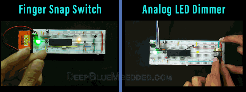
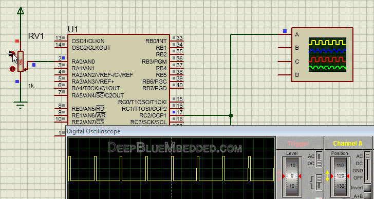
LED Dimmer – ADC LAB1
| Lab Name | Analog Input – Analog Output (LED Dimmer) – ADC+PWM |
| Lab Number | 21 |
| Lab Level | Beginner |
| Lab Objectives | Learn how to configure The ADC Module and read analog signals. Combine the analog readings from a potentiometer with PWM to control LED brightness. |
1. Coding
Open the MPLAB IDE and create a new project name it “ADC_LED_Dimmer”. If you have some issues doing so, you can always refer to the previous tutorial using the link below.

Set the configuration bits to match the generic setting which we’ve stated earlier. And if you also find troubles creating this file, you can always refer to the previous tutorial using the link below.
Now, open the main.c file and let’s start developing the firmware for our project.
The first task is to initialize the ADC and PWM modules using the basic firmware drivers which we’ve already built previously. Then, we’ll read convert the voltage level on Analog Channel 0 and send the 10-Bit A/D conversion result as a Duty Cycle for PWM1. So the brightness of the LED is determined by the analog input for Channel 0.
Here is the Full Code Listing For This LAB
|
1 2 3 4 5 6 7 8 9 10 11 12 13 14 15 16 17 18 19 20 21 22 23 24 25 26 27 28 29 30 31 32 33 34 35 36 37 38 39 40 41 42 43 44 45 46 47 48 49 50 51 52 53 54 55 56 57 58 59 60 61 62 63 64 65 66 67 68 69 70 71 72 73 74 75 76 77 |
/* * LAB Name: ADC LED Dimer * LAB Num.: 21 * Author: Khaled Magdy * Visit My Website @ DeepBlueMbedded.com */ #include <xc.h> #include "config.h" #include <stdint.h> #define _XTAL_FREQ 4000000 //-----[ Prototypes ]---- void PWM1_Init(); void PWM1_Set_Duty(uint16_t); void ADC_Init(); uint16_t ADC_Read(uint8_t); //==================================================== //----------[Main Routine]------------- void main(void) { PWM1_Init(); ADC_Init(); while(1) { PWM1_Set_Duty(ADC_Read(0)); // Set PWM Duty Cycle To AN0_Result! __delay_ms(1); } return; } //----------[END OF MAIN]------------- //==================================================== //------------[ CCP/PWM Routines ]-------------- void PWM1_Init() { //--[ Configure The CCP Module For PWM Mode ]-- CCP1M3 = 1; CCP1M2 = 1; TRISC2 = 0; // The CCP1 Output Pin (PWM) // Set The PWM Frequency (5kHz) PR2 = 124; // Set The PS For Timer2 (1:4 Ratio) T2CKPS0 = 1; T2CKPS1 = 0; // Start CCP1 PWM ! TMR2ON = 1; } void PWM1_Set_Duty(uint16_t DC) { // Check The DC Value To Make Sure it's Within 10-Bit Range if(DC<1024) { CCP1Y = DC & 1; CCP1X = DC & 2; CCPR1L = DC >> 2; } } //------------[ AD Converter Routines ]-------------- void ADC_Init() { ADCON0 = 0x41; // Turn ADC ON, Select AN0 Channel, ADC Clock = Fosc/8 ADCON1 = 0x80; // All 8 Channels Are Analog, Result is "Right-Justified" // ADC Clock = Fosc/8 } uint16_t ADC_Read(uint8_t ANC) { if(ANC<0 || ANC>7) // Check Channel Number Validity { return 0;} ADCON0 &= 0b11000101; // Clear The Channel Selection Bits ADCON0 |= ANC<<3; // Select The Required Channel (ANC) // Wait The Aquisition Time __delay_us(30); // The Minimum Tacq = 20us, So That should be enough GO_DONE = 1; // Start A/D Conversion while(ADCON0bits.GO_DONE); // Polling GO_DONE Bit // Provides Delay Until Conversion Is Complete return ((ADRESH << 8) + ADRESL); // Return The Right-Justified 10-Bit Result } |
2. Simulation
Here is an animation for the running simulation tests.
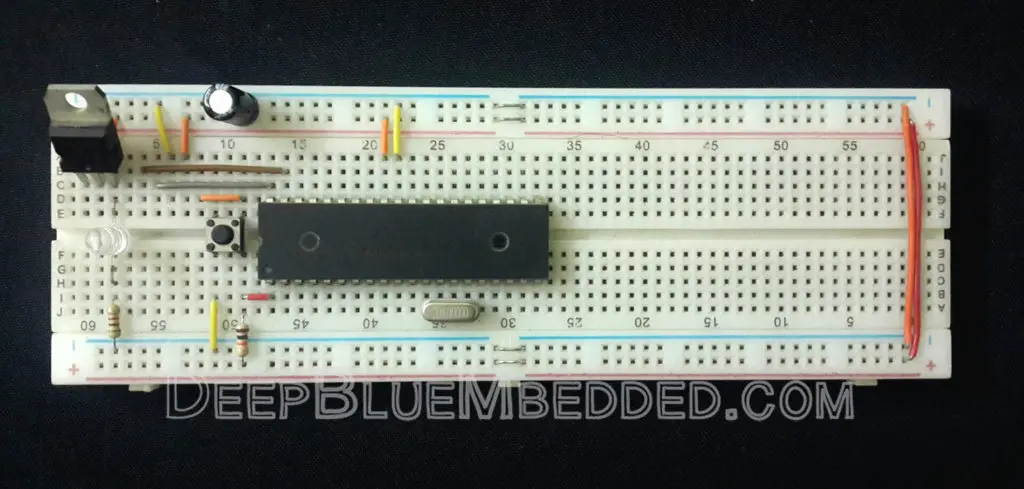
3. Prototyping
Wiring up this schematic on a breadboard should be an easy task. Just upload your firmware hex file to the microcontroller chip. And hook up the input power rails and start testing it up!
Here is a video for the final output of this LAB.
If you’ve any troubles or got stuck at any point, just drop me a comment. I’ll be always here and ready for help. Or even other readers may do a better job in this.
Finger Snap Switch – ADC LAB2
| Lab Name | Finger Snap Switch |
| Lab Number | 22 |
| Lab Level | Intermediate |
| Lab Objectives | Learn how to configure The ADC module and read analog signals. Identify sound intensity (loudness) in order to flip a LED when a finger snap is captured by a microphone! |
1. Coding
Open the MPLAB IDE and create a new project name it “ADC_Microphone”. If you have some issues doing so, you can always refer to the previous tutorial using the link below.
Set the configuration bits to match the generic setting which we’ve stated earlier. And if you also find troubles creating this file, you can always refer to the previous tutorial using the link below.
Now, open the main.c file and let’s start developing the firmware for our project.
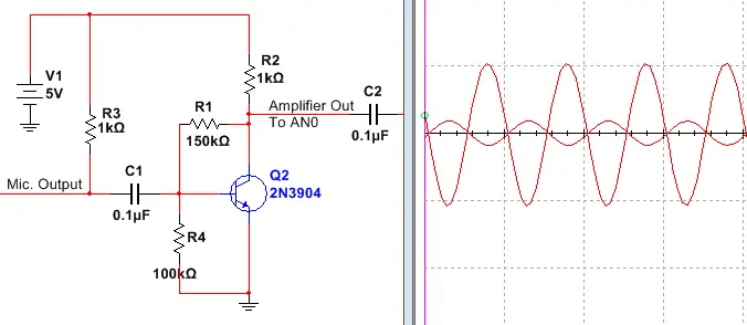
The first task is to initialize the ADC module using the basic firmware driver which we’ve already built previously. Then, we’ll continuously convert & read the voltage level on Analog Channel 0 (The Microphone Amplified Output) and compare 10-Bit A/D conversion against a specific threshold value. So we can detect any loud sound nearby and flip an LED as a result.
Here is The Full Code Listing For This Project
|
1 2 3 4 5 6 7 8 9 10 11 12 13 14 15 16 17 18 19 20 21 22 23 24 25 26 27 28 29 30 31 32 33 34 35 36 37 38 39 40 41 42 43 44 45 46 47 48 49 50 51 52 53 54 55 56 57 58 59 |
/* * LAB Name: ADC Microphone (Finger Snap Switch) * LAB Num.: 22 * Author: Khaled Magdy * Visit My Website @ DeepBlueMbedded.com */ #include <xc.h> #include "config.h" #include <stdint.h> #define _XTAL_FREQ 4000000 //-----[ Prototypes ]---- void ADC_Init(); uint16_t ADC_Read(uint8_t); //==================================================== //----------[Main Routine]------------- void main(void) { uint16_t AN0_RES = 0, TH = 850; // You'll Have To Figure Out // The Best Threshold Value For You ADC_Init(); // Initialize ADC Module TRISC7=0; // IO Output Pin (LED) RC7=0; // Initially OFF while(1) { AN0_RES = ADC_Read(0); // Read Analog Channel 0 if(AN0_RES > TH) { RC7 = ~RC7; __delay_ms(10); } __delay_ms(1); } return; } //----------[END OF MAIN]------------- //==================================================== //------------[ AD Converter Routines ]-------------- void ADC_Init() { ADCON0 = 0x41; // Turn ADC ON, Select AN0 Channel, ADC Clock = Fosc/8 ADCON1 = 0x80; // All 8 Channels Are Analog, Result is "Right-Justified" // ADC Clock = Fosc/8 } uint16_t ADC_Read(uint8_t ANC) { if(ANC<0 || ANC>7) // Check Channel Number Validity { return 0;} ADCON0 &= 0b11000101; // Clear The Channel Selection Bits ADCON0 |= ANC<<3; // Select The Required Channel (ANC) // Wait The Aquisition Time __delay_us(30); // The Minimum Tacq = 20us, So That should be enough GO_DONE = 1; // Start A/D Conversion while(ADCON0bits.GO_DONE); // Polling GO_DONE Bit // Provides Delay Until Conversion Is Complete return ((ADRESH << 8) + ADRESL); // Return The Right-Justified 10-Bit Result } |
Note!
Note: You should know that the output audio signal captured by the microphone will be a few milli-volts in magnitude! That’s almost identical to the resolution of our ADC, therefore it’s impossible to capture such a signal. Hence, we’ll have to build a very basic amplifier to give this signal a constant gain. Here is the simplest common-emitter amplifier that you can build with a transistor and a few resistors.
2. Prototyping
And here is a video for the final output of this LAB.
If you’ve any troubles or got stuck at any point, just drop me a comment. I’ll be always here and ready for help. Or even other readers may do a better job in this.
Different Schemes To Read ADC
Single Channel Conversion
1 One Shot
The one-shot scheme of conversion is basically what we’ve done so far in a previous couple of LABs. The A/D converter is activated and ready for conversion, and if you need to convert a specific analog channel, you’ll call the ADC_Read routine. Consequently, the A/D will switch over to the desired analog channel and a conversion process will be initiated until the result is ready.
This scheme can be used for many applications, specifically low power applications. Which requires low sampling rate A/D conversion. You can set up a timer interrupt and initiate A/D conversions as periodic one-shot conversions.
Sometimes, this scheme will not be sufficient by any means. And I confirm that your ADC is capable of more! it can produce a much higher sampling rate if your application needs to.
|
1 |
AN_RES = ADC_Read(ANx); // One-Shot A/D Conversion! |
2 Continuous Mode
This mode is an automatic self-triggering continuous series of A/D conversions. In this way, you’ll push your ADC to its limits and go far near the maximum sampling rate possible.
You can set up A/D interrupt and self-trigger the ADC after reading each sample. As you know, switching channels require waiting some time which is something that you don’t want. Provided that your target is to shoot for the maximum possible A/D sampling rate.
To give you an idea of how this can be implemented, here is a code snippet for the ISR in this case
|
1 2 3 4 5 6 7 8 9 10 11 12 |
void __interrupt() ISR(void) { if(ADIF) { // Read A/D Conversion Result Registers ADRESH, ADRESL AN_RES = (ADRESH << 8) + ADRESL; // Clear The ADC Interrupt Flag Bit ADIF = 0; // Start New Conversion! GO_DONE = 1; } } |
Please, be advised that this scheme maximizes your overall ADC’s sampling rate. However, you should know that you’re sacrificing CPU time which is going to be overloaded by the excessive amount of interrupts. This “interrupts jitter” is obviously proportional to the current sampling rate of your ADC + any other interrupt sources!
Multiple Channels Conversion
1 Burst of Conversions
In some situations, your microcontroller will have to read multiple analog channels. And as we know that there is only 1 A/D resource. That’s why we have to configure the analog channel selection switch before issuing an A/D conversion.
One way to get this task done is to do a burst of conversions in a row for all your analog channels. In this way, you’ll be able to sequentially convert all your channels in a row. Here is a typical implementation for a burst conversion routine.
|
1 2 3 4 5 6 7 8 9 10 11 12 13 14 |
void ADC_Burst(uint16_t* AN_RES_BUF, uint8_t N) { for(uint8_t i = 0; i<N; i++) { ADCON0 &= 0x11000101; // Clear The Channel Selection Bits ADCON0 |= i<<3; // Select The Required Channel (i) // Wait The Aquisition Time __delay_us(30); // The Minimum Tacq = 20us, So That should be enough GO_DONE = 1; // Start A/D Conversion while(ADCON0bits.GO_DONE); // Polling GO_DONE Bit // Provides Delay Until Conversion Is Complete AN_RES_BUF[i] = ((ADRESH << 8) + ADRESL); } } |
2 Continuous Bursts
Obviously, you can set up the A/D converter interrupt signal in order to continuously update your analog channels result buffer sequentially. And the “interrupt jitter” problem will also arise in this case.
Concluding Remarks
1
How To Measure Voltage Greater Than Vcc (>5v)
You can just attenuate the original signal by using a proper attenuator or maybe a voltage divider! a couple of resistors will give your ADC much higher upper limit for conversion.
Using R & R resistors, you’ll make your ADC capable of reading up to 10volts. Similarly, using R & 3R, you’ll be able to read signals up to 20volts. Just Apply Voltage Divider Rule.
What you should notice is the fact that the accuracy is dropping significantly as we go up. The lower the voltage is, the less error generated by the A/D measurement setup.
2
How To Measure Small Signals (~mv)
Designing a suitable amplifier for your system will make the job of A/D converter much easier. Sometimes a simple common emitter amplifier will do the trick. Even an op-amp can do much help.
However, sometimes you may need something different. Here is an example, instead of trying to measure too very small signals to check the difference between them. You just can use a differential amplifier and amplify this difference between the signals. Now the job of our ADC is much easier than before! And so on…
3
Converting ADC Result Back To Voltage
After a successful A/D conversion, you can work it in reverse to calculate back the original voltage level. This only requires the knowledge of your ADC’s current resolution Q.
For 10-Bit ADC with FSR=5v, assume a digital result of conversion ANRES = 256
Then the analog corresponding voltage is calculated as shown below
![]()
![]()
Was this helpful for you? Why not share it with your network! it took too much time and effort in order to craft such a piece of content. Sharing is the best way for supporting free technical content like this,
Regards,
Khaled M.
| Previous Tutorial | Tutorial 22 | Next Tutorial | |||||
In the first example I have tried i am really confused on how you are directly giving the 10 bit ADC value to Duty cycle, I know that duty cycle is also 10 bit but it is maxing out around 500(0-1023 scale).
I used a 20 MHz PIC MCU, 10KHz freq, so PR = 124,PS = 4
The other difference is ADCON0 = 0x81; ADCON1 = 0x80; (20MHz)
The rest of code is the same
until half of the POT the duty changes as expected, but beyond that it becomes messy waveform.
Please help…
Well,if that is the case for your program you can right shift the AD-result once so you can fit in the 9bit duty cycle.
The resolution for pwm duty cycle is bot fixed. Its max is 10bits however, and for high pwm freq, it’s going to be much less. Maybe 8bits or something depending on the exact freq value using the resolution formula you can find that easily.
For me the PWM output values change from 0 – 1024 as expected but the pot moves only till half, so i divided the ADC by half to match the : CCPR1L = 0(0% duty)-500(100% duty) and it worked (Except when the ADC is above 1000)
” PWM1_Duty(ADC_Read(0)/2);
void PWM1_Duty(uint16_t DC){
if (DC>2;
}
}
”
I know that this is not the actual way to approach the mapping
Could you tell me a better way to map the ADC values to the PWM equivalent without using a cascade of if else loops….
Thanks a lot
You’re totally true. It’s not the way to go, so you’ve got to do the mapping using the method i’ve shown in the concluding remarks or in the final lab as well. Just look at the figure where i did deduce the mapping formula for the case of that lab. And you’ll get an idea of how to do it for your application.
Hello Khaled,
Thanks for your detailed explanation of the PIC ADC. I have a question about the following portion of the coding, if you can explain this portion to me. Questions in the asterisk **
if(ANC7) // Check Channel Number Validity *this part no problem at all*
{ return 0;}
ADCON0 &= 0b11000101; // Clear The Channel Selection Bits *what is its purpose & how it works, why the & sign*
ADCON0 |= ANC
ADCON0 &= 0b1100010 , the purpose of this instruction is to make CHS0,CHS1 and CHS2 = 0 . to clear the selection of the channel from the last reading.
ADCON0 |= ANC
Hello Khaled.I wonder something about of this while(ADCON0bits.GO_DONE); line of code from lab 1.
From what I understand,if the expression inside the parenthesis evaluates to 0, then compiler does not go to the next line of code and waits until this expression inside the parenthesis evaluates to 1.İf expression evaluates to one it continues to execute the next lines.
Still I am not sure if I am right or wrong.Can you explain What this line does?
Respected Sir !
I wanted to be an embedded engineer. At moment I am in 6th semester however I do not know from where should I start please guide me.