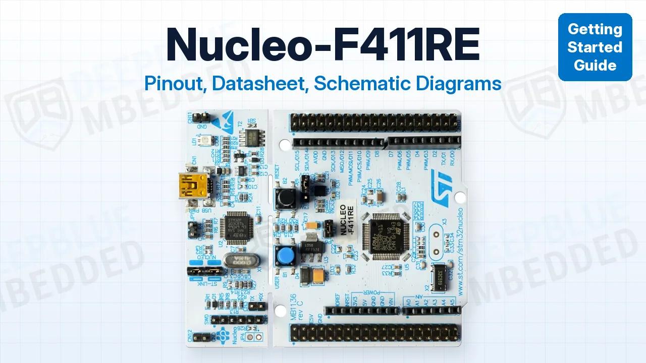
In this guide, you’ll find the Nucleo-F411RE pinout diagram, its datasheet and schematic diagram, and every pin group explained with its default pins and gotchas. Without further ado, let’s get right into it!
The Nucleo-F411RE is ST’s official Nucleo-64 board for the STM32F411RE, a 100MHz Arm Cortex-M4 with FPU, 512KB Flash and 128KB RAM. It gives you 50 GPIO pins on the Arduino Uno and ST Morpho headers, 5 SPI ports, USB OTG, and an on-board ST-LINK debugger, so all you need is a USB cable. It’s the exact same MB1136 PCB as the Nucleo-F401RE and the Nucleo-F446RE; only the MCU is different.
Nucleo-F411RE Pinout Diagram
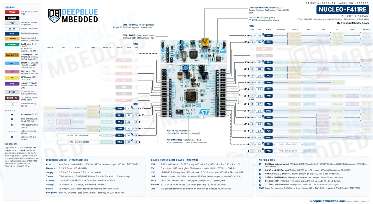
Here is a detailed Nucleo-F411RE Pinout Diagram with colored labels and legends to help you easily identify the functionalities that each pin can perform. This first diagram covers the Arduino Uno V3 headers (CN5, CN6, CN8, and CN9), which is where most shields and jumper wires go.
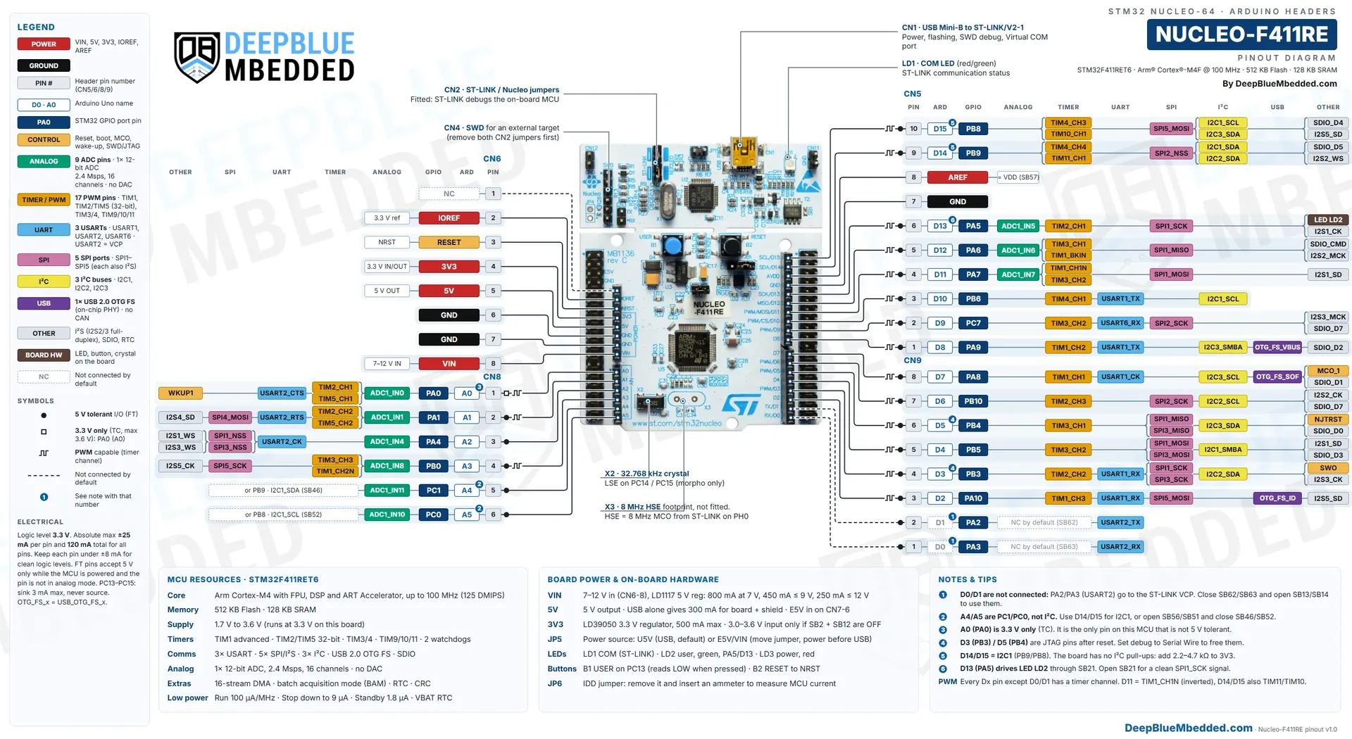
Each row shows the header pin number, the Arduino name (D0–D15, A0–A5), the STM32 GPIO name and its alternate functions, color-coded by peripheral. The small dot marks a 5v-tolerant pin and the small square marks the only 3.3v-only pin (A0, PA0). The dashed lines mark pins that aren’t connected by default, and the numbered badges point to the notes at the bottom of the diagram.
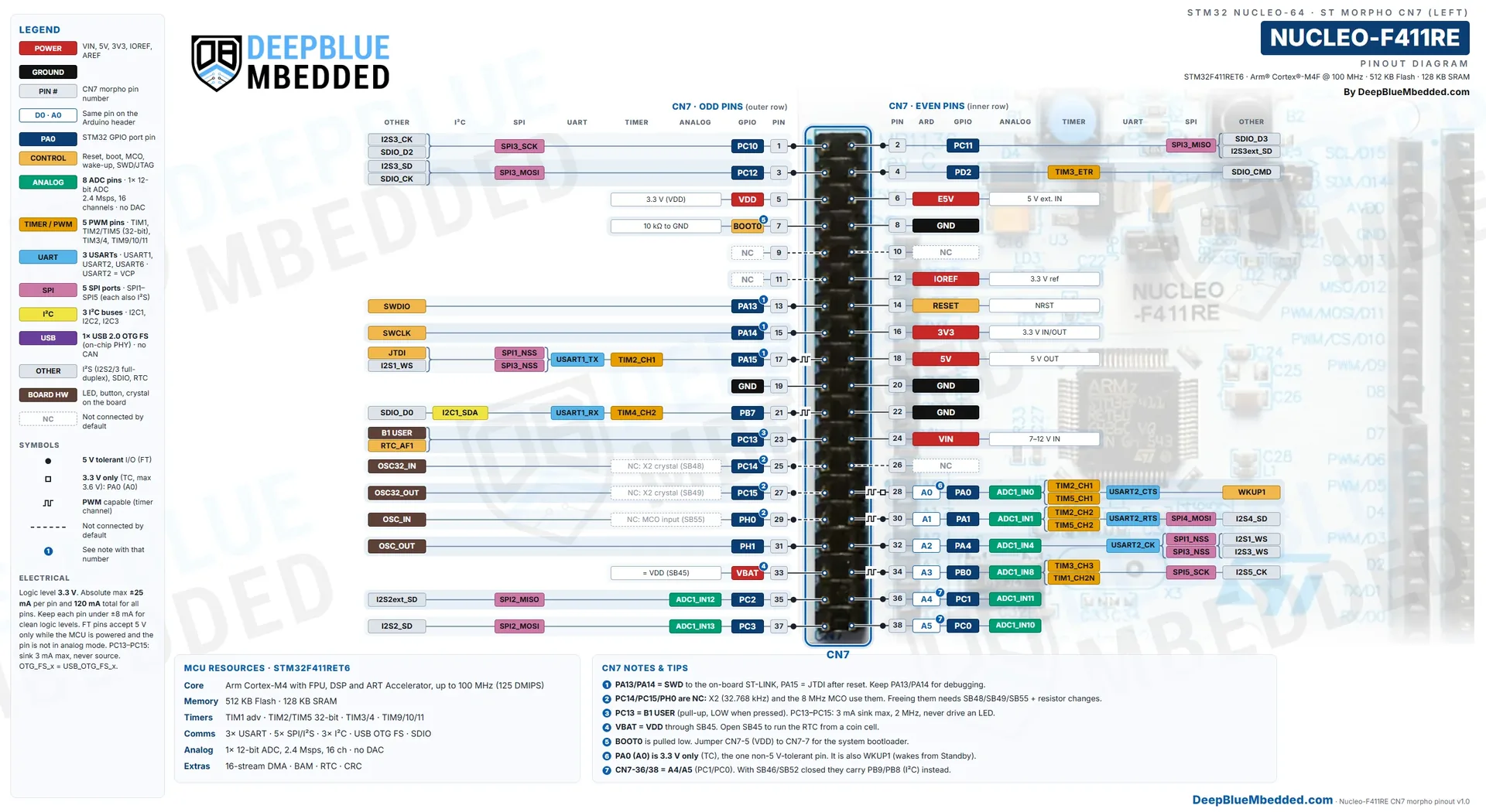
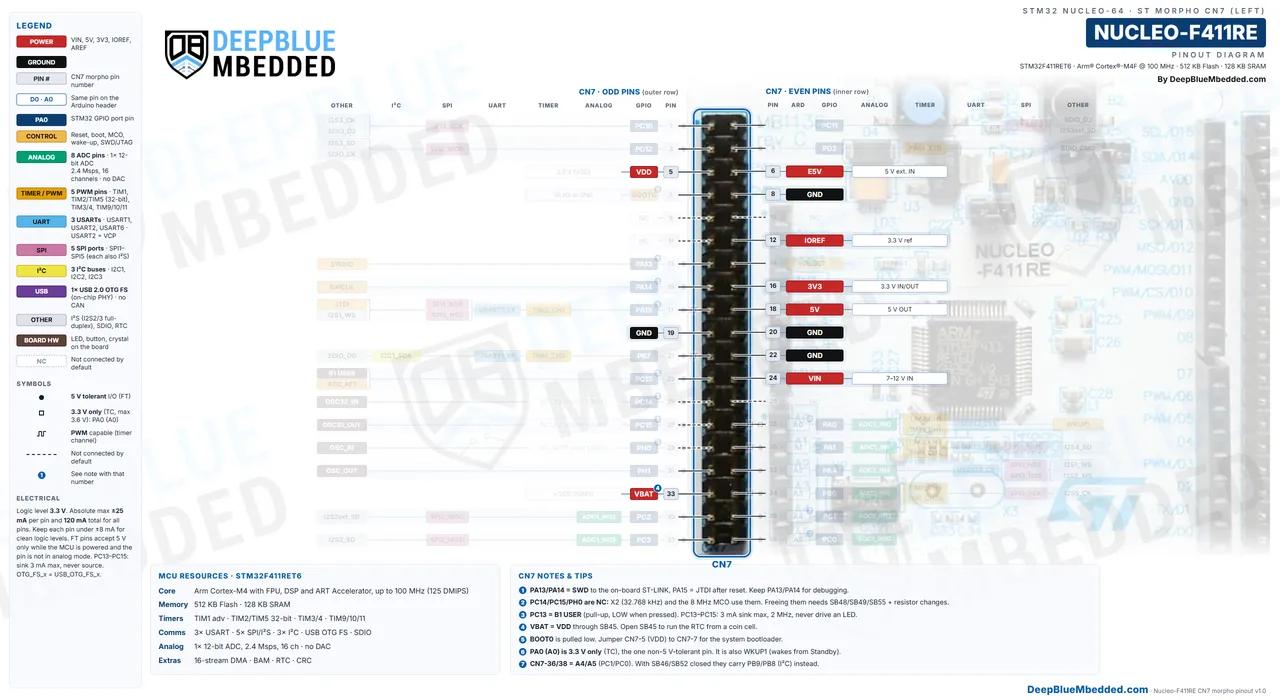
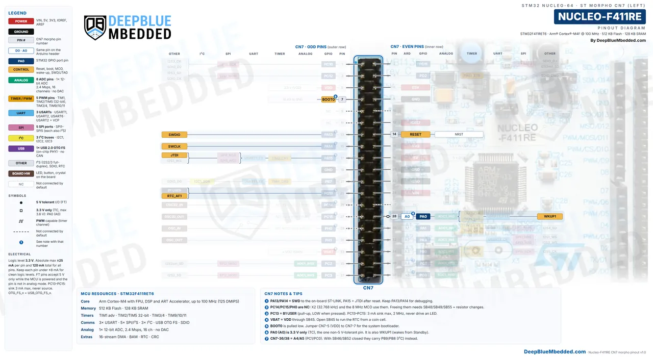
Nucleo-F411RE Morpho CN7 Pinout
The left ST Morpho header CN7 is a 2×19 male header. Odd pins (1, 3, 5…37) are on the outer column and even pins are on the inner column, with pin 1 at the top, next to the ST-LINK part of the board.
Nucleo-F411RE Morpho CN10 Pinout
The right ST Morpho header CN10 is also 2×19, but here the odd pins are on the inner column. It carries the extra peripherals of the F411 that the Arduino headers don’t have, like the USB OTG FS data pins (PA11/PA12), SPI2, SPI4, SPI5 and USART6.
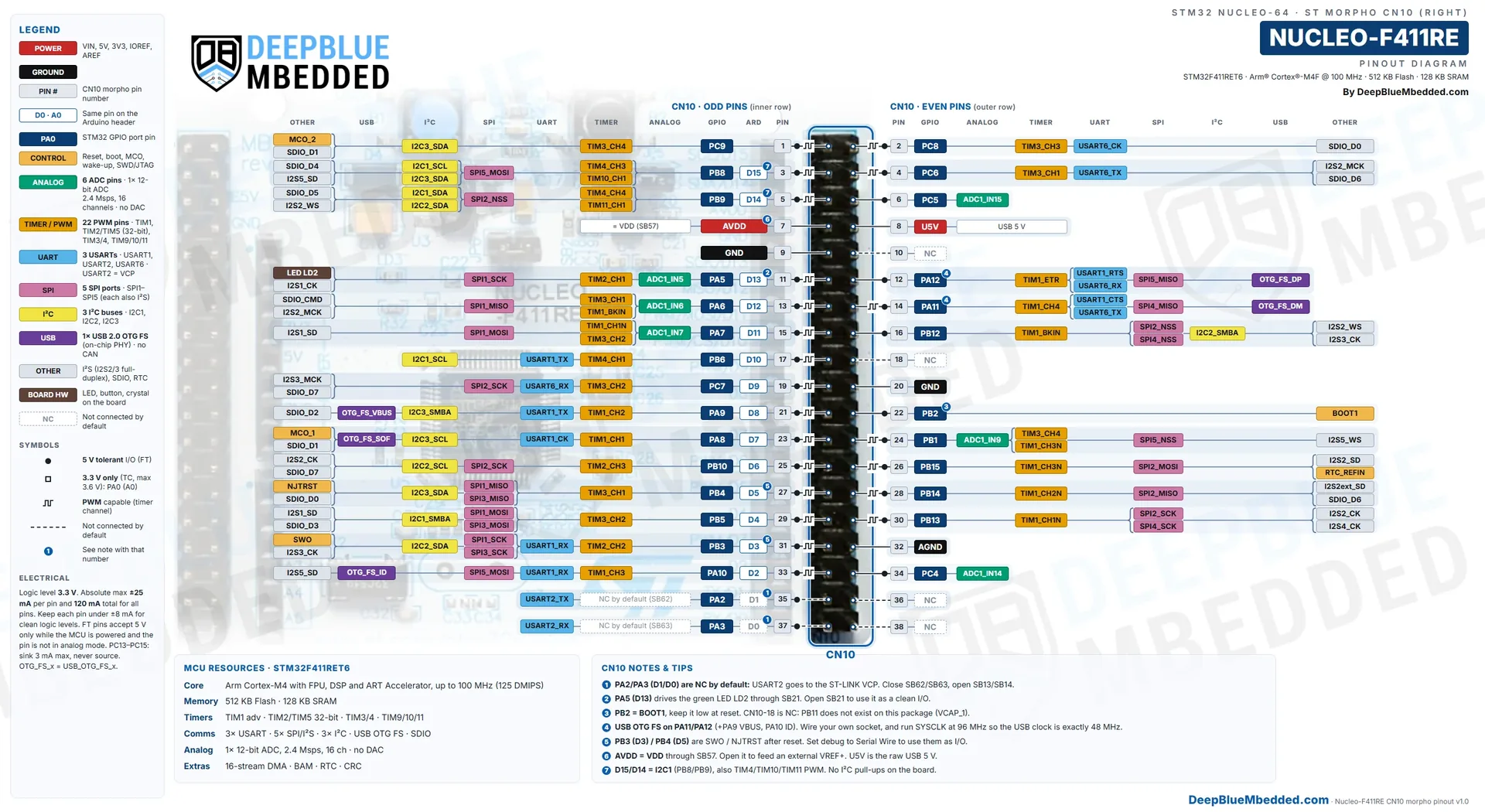
Note that every Arduino header signal is also present on the Morpho headers (for example, D13/PA5 is also CN10-11), so the Morpho headers are a superset: all 50 GPIOs of the STM32F411RE are on CN7 and CN10.
Buy a Nucleo-F411RE: If you don’t have one yet, you can get the official ST board from Amazon or AliExpress. It comes with the ST-LINK debugger on board, so you can start programming it right away.
Download Nucleo-F411RE Pinout Diagrams (Full Resolution)
All 3 Nucleo-F411RE pinout diagrams (Arduino headers, CN7 and CN10 morpho) in full resolution (5120×2800 px WebP), in one ZIP file. Print them, zoom in, or keep them next to your bench. Please consider supporting my work if it helped you.
Nucleo-F411RE Datasheet
This development board is built around the STM32F411RET6 microcontroller (LQFP64 package). Here are the official Nucleo-F411RE datasheet and documents you’ll need for it, all linked to ST’s own servers so you always get the latest revision:
| Document | ID | Revision | What you’ll use it for | Link |
|---|---|---|---|---|
| STM32F411xC/xE datasheet | DS10314 | Rev 8 (Jan 2024) | Pin definitions (FT/TC), alternate-function table, electrical limits | |
| STM32F411xC/E reference manual | RM0383 | Rev 4 (Jun 2025) | Registers and how every peripheral works | |
| STM32 Nucleo-64 boards (MB1136) user manual | UM1724 | Rev 17 (Sep 2025) | Board pinout tables, jumpers, solder bridges, power options | |
| STM32 Nucleo-64 boards data brief | DB2196 | Rev 23 (Oct 2026) | One-page board summary and order codes | |
| STM32F411xC/xE errata sheet | ES0287 | Rev 6 (Feb 2025) | Known silicon limitations and workarounds | |
| System memory boot mode (bootloader) | AN2606 | Rev 71 (Nov 2026) | Which pins the built-in bootloader listens on (section 38) | |
| MB1136 board schematic | MB1136 C-04 | Aug 2022 | Full board circuit (see the next section) |
Which document do I need? The datasheet for pin functions and electrical limits, the reference manual for registers, and the UM1724 user manual for jumpers, solder bridges, and the header map. The board documents are on the official NUCLEO-F411RE product page, and the chip documents on the STM32F411RE product page.
Nucleo-F411RE Schematic
The Nucleo-F411RE schematic is shown below, which covers every Nucleo-64 board form factor, including the F411RE.
Here are its 4 schematic sheets; click a page to view it full screen.
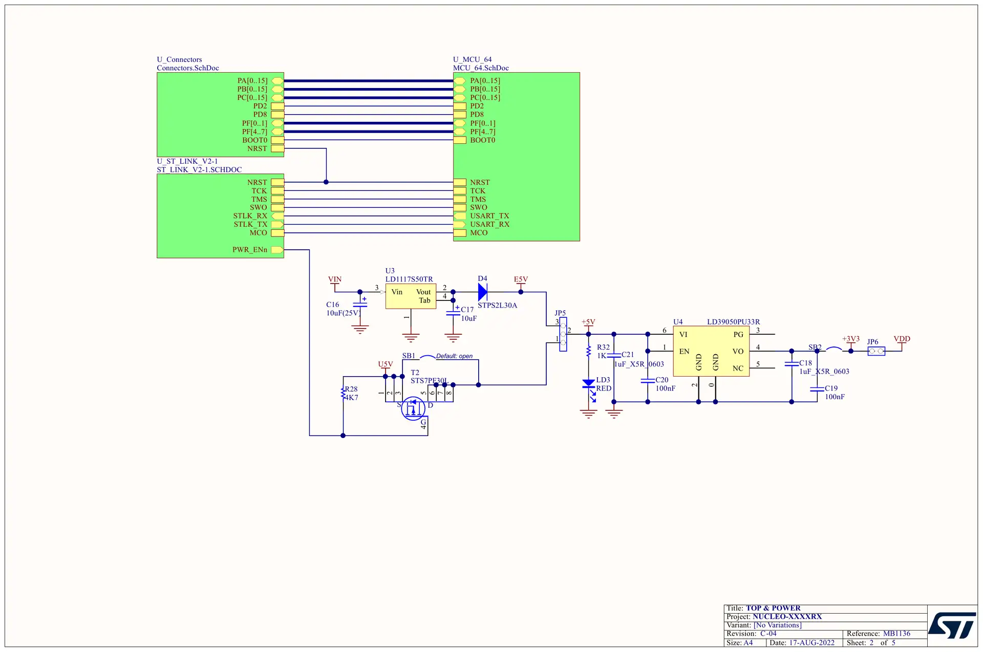
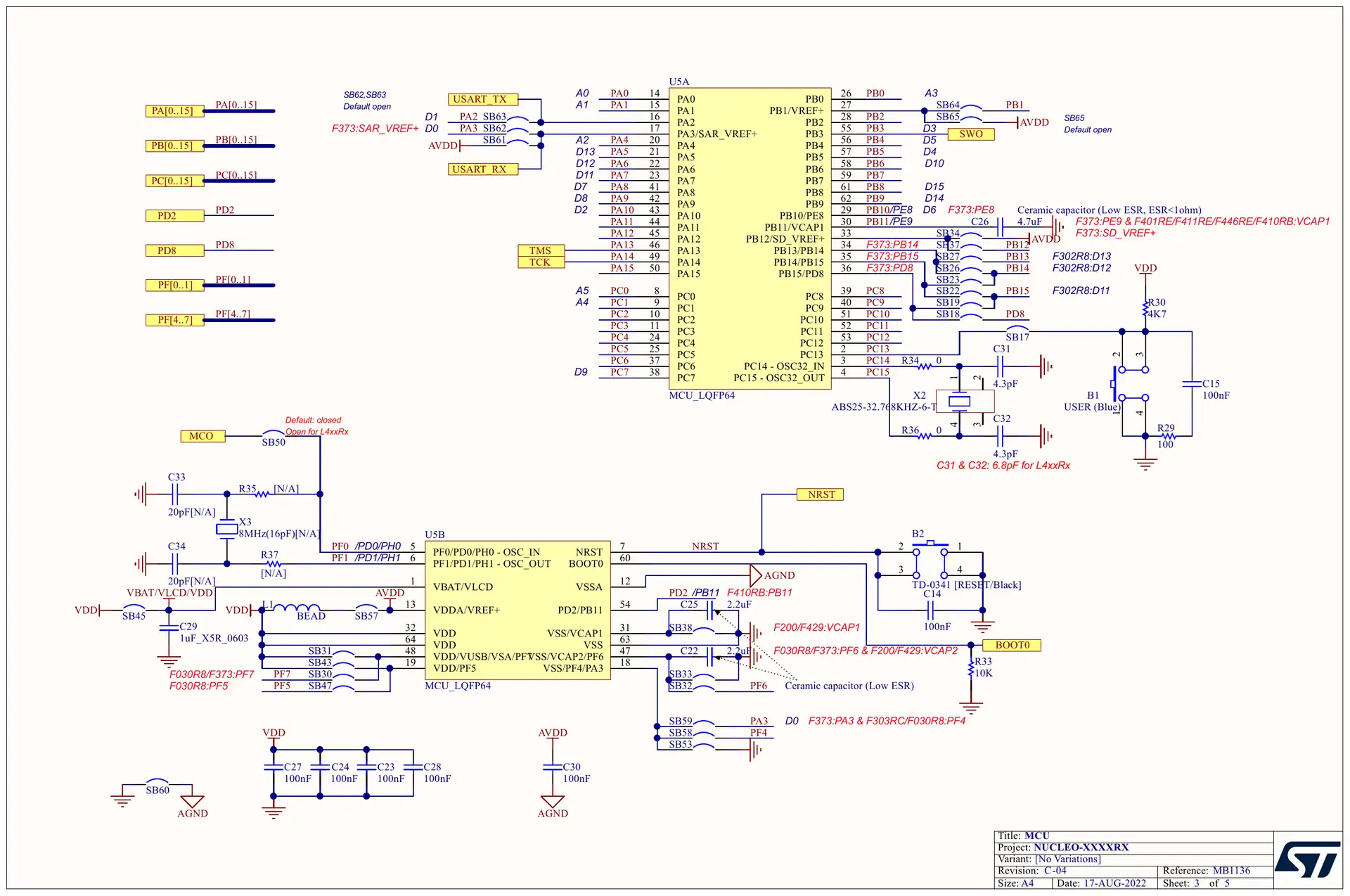
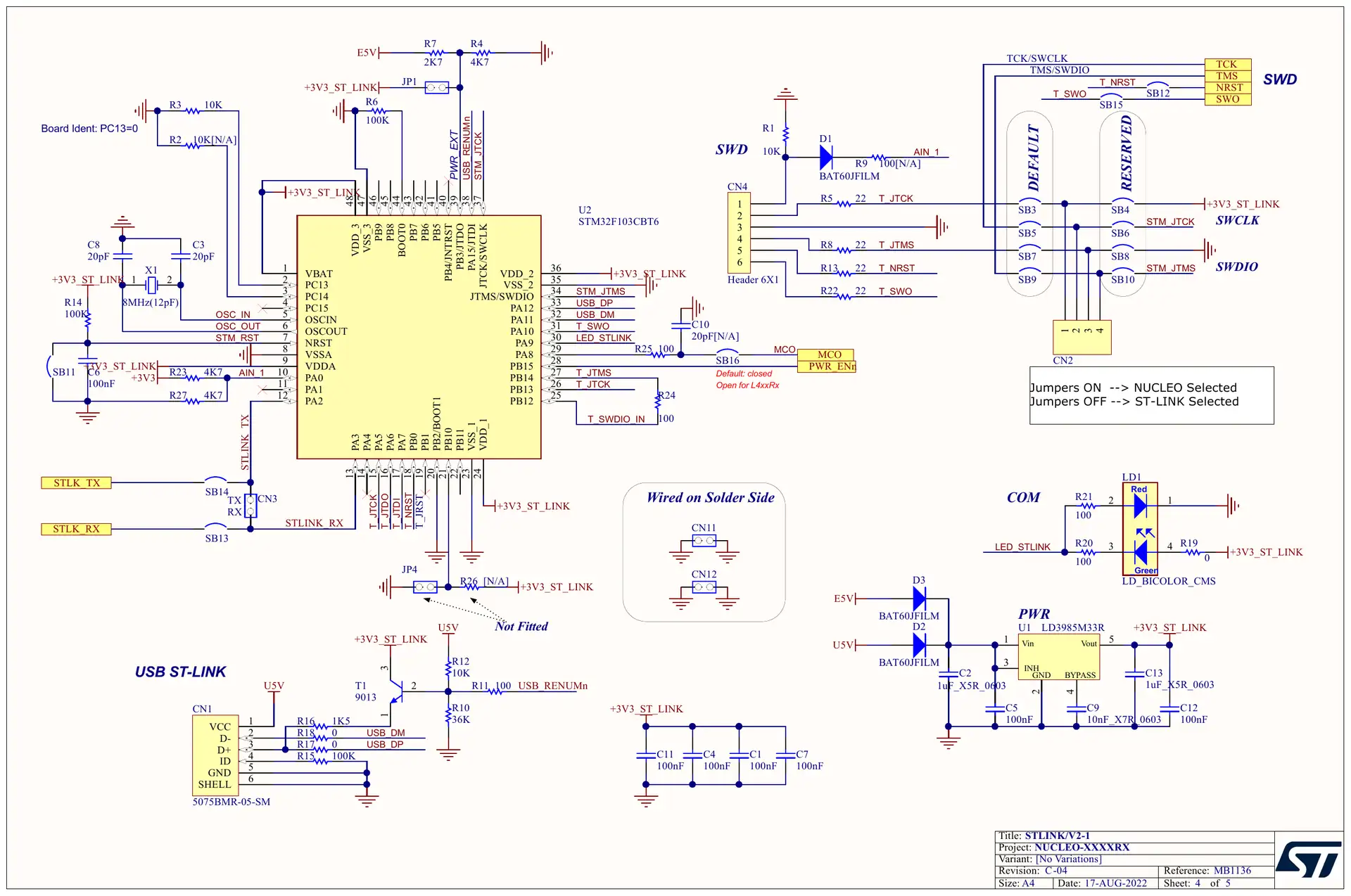
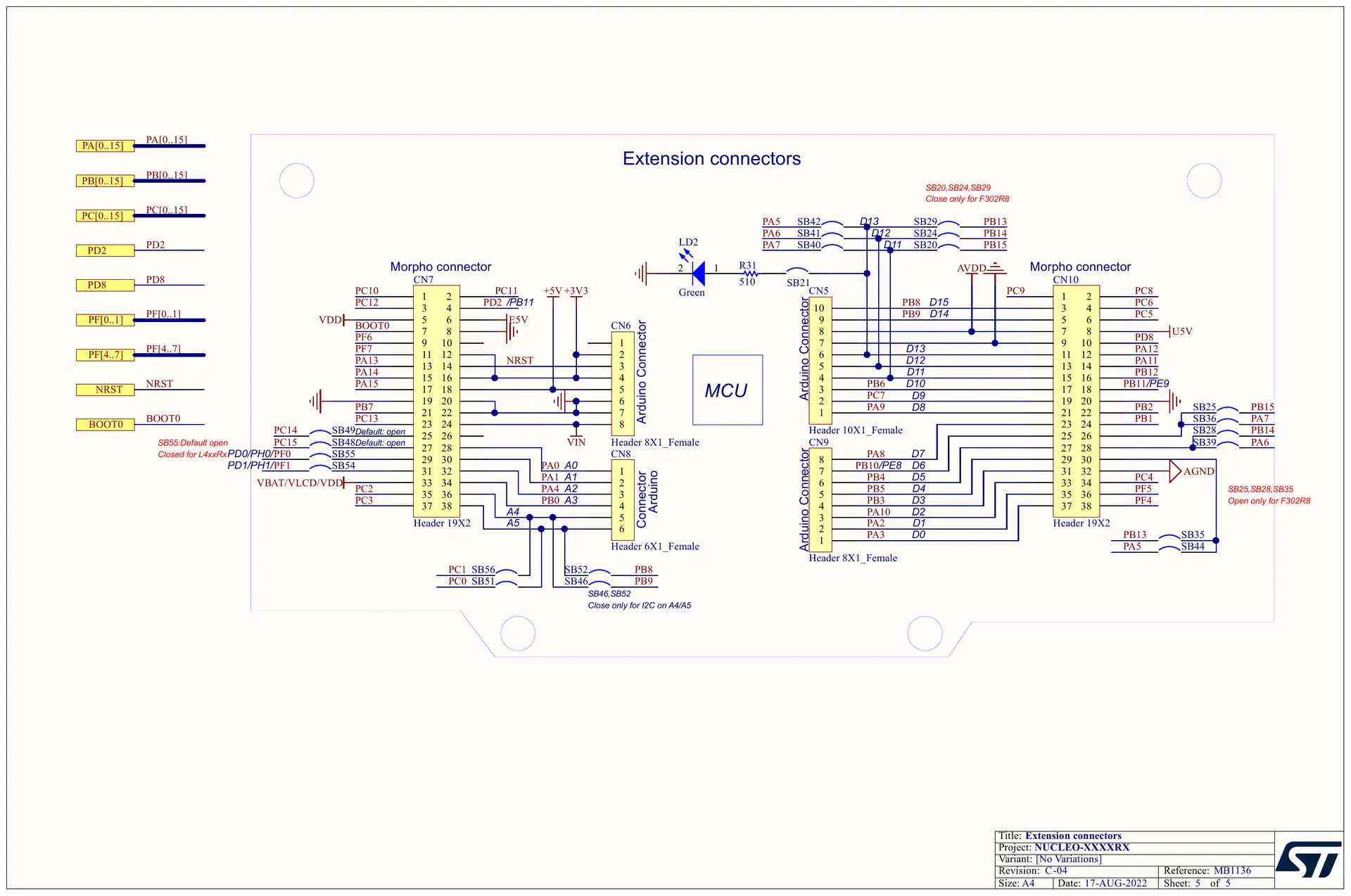
Official source: MB1136 C-04 schematic (PDF) from the NUCLEO-F411RE product page (CAD Resources). Here’s what to look at on each sheet:
- Power path (sheet 1): USB 5v (U5V) goes through a power switch that the ST-LINK turns on only after the PC grants 300mA. VIN (7v–12v) feeds the LD1117S50 5v regulator, and jumper JP5 picks U5V or E5V. The 5v rail then feeds the LD39050PU33R 3.3v regulator (500mA) that powers the MCU.
- Solder bridges (sheet 2): SB13/SB14 route PA2/PA3 to the ST-LINK Virtual COM port, SB62/SB63 (open) keep them off D1/D0, SB51/SB56 put PC0/PC1 on A5/A4, and SB21 connects LD2 to PA5.
- Clocks (sheet 2): there’s no 8MHz crystal on the MCU side. X3 is not fitted, and the ST-LINK feeds an 8MHz MCO clock into PH0 (SB16, SB50). The 32.768kHz crystal X2 sits on PC14/PC15 for the RTC.
- ST-LINK/V2-1 (sheet 3): an STM32F103CBT6 does the SWD debugging (PA13/PA14, PB3 SWO, NRST), the USB mass-storage flashing, and the Virtual COM port. Removing the two CN2 jumpers frees it to debug an external board on CN4.
- Extension connectors (sheet 4): the Arduino (CN5/CN6/CN8/CN9) and Morpho (CN7/CN10) headers, with every solder-bridge option drawn next to the pin it changes.
Nucleo-F411RE Specs
The Nucleo-F411RE combines a 100MHz STM32F411RET6 with the standard Nucleo-64 board (MB1136 rev C). Here are its specifications, including the board-level parts that chip-only spec lists usually skip.
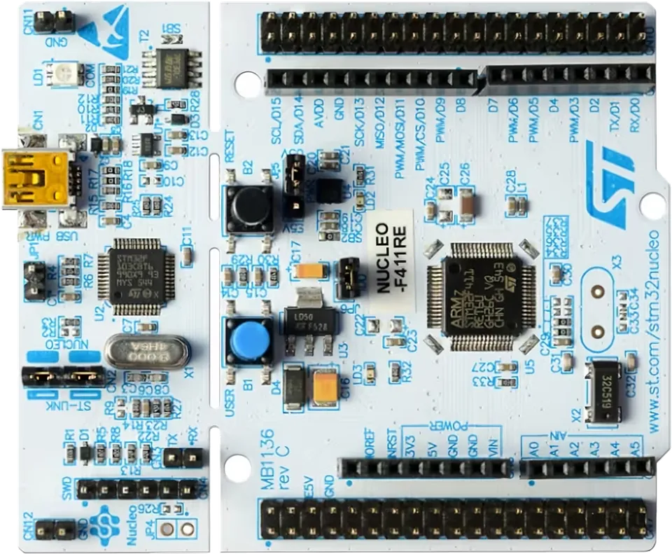
Get a Nucleo-F411RE: The official ST board is the one I recommend. Grab it from Amazon or AliExpress.
| Item | Nucleo-F411RE |
|---|---|
| MCU | STM32F411RET6, LQFP64 |
| Core | Arm Cortex-M4 with FPU and DSP, up to 100MHz (125 DMIPS), ART Accelerator |
| Memory | 512KB Flash, 128KB SRAM |
| Logic level | 3.3v (every I/O pin is 5v tolerant except PA0/A0) |
| GPIO pins | 50 on the Morpho headers, 22 on the Arduino headers (20 connected by default) |
| Board supply | USB 5v (300mA), VIN 7v–12v, E5V 4.75v–5.25v, or 3.3v direct |
| 5v regulator | LD1117S50TR: 800mA at 7v in, 450mA at 7v–9v, 250mA at 9v–12v |
| 3.3v regulator | LD39050PU33R, 500mA |
| Clocks | 8MHz MCO from the ST-LINK into PH0 (HSE bypass), 32.768kHz LSE crystal (X2); X3 HSE crystal not fitted |
| Debugger | On-board ST-LINK/V2-1 (snap-off): SWD, drag-and-drop flashing, Virtual COM port on USART2 |
| USB connector | Mini-B (CN1), for the ST-LINK only |
| Headers | Arduino Uno V3 (CN5, CN6, CN8, CN9) + two 2×19 ST Morpho headers (CN7, CN10) |
| User I/O | LD2 green LED (PA5), B1 user button (PC13), B2 reset button |
| Low power (MCU) | 100µA/MHz in Run, 42µA in Stop (down to 9µA with Flash in deep power down), 1.8µA in Standby (typical, from DS10314) |
| PCB | MB1136 rev C, the same PCB as the Nucleo-F401RE and F446RE |
Nucleo-F411RE Specifications Summary
- The Nucleo-F411RE runs the STM32F411RET6 at up to 100MHz with 512KB Flash and 128KB RAM.
- All 50 GPIOs are on the Morpho headers; the Arduino headers carry 22 of them (D0/D1 are disconnected by default).
- Every I/O pin is 5v tolerant except PA0 (A0), which is a 3.3v-only (TC) pin. Any pin in analog mode is 3.3v-only too.
- It has 1x 12-bit ADC (2.4Msps) with 16 external channels; 9 ADC pins are on the Arduino headers (A0–A5, D11–D13).
- There is no DAC and no CAN on the STM32F411RE.
- 17 Arduino pins can output PWM: D2–D15, A0, A1 and A3. D11 is the complementary channel TIM1_CH1N.
- It has 3 USARTs (USART1, USART2, USART6). USART2 on PA2/PA3 is the ST-LINK Virtual COM port, not D0/D1.
- The default I2C pins are D15 (PB8, SCL) and D14 (PB9, SDA); A4/A5 are not I2C by default.
- It has 5 SPI ports (SPI1–SPI5); the default SPI pins are D13 (SCK), D12 (MISO), D11 (MOSI) on SPI1.
- USB OTG FS is on PA11 (D−) and PA12 (D+), on the Morpho header CN10 only, and needs a 96MHz system clock (not 100MHz) for an exact 48MHz USB clock.
- The user LED LD2 is on PA5 (D13), and the user button B1 is on PC13.
- VIN accepts 7v–12v, and the 3.3v regulator gives up to 500mA.
Nucleo-F411RE Peripherals: MCU vs On the Headers
The STM32F411RE has more peripherals than the Arduino headers can show. This table tells you what the chip has and where you can actually reach it on the board.
| Peripheral | STM32F411RE (LQFP64) | On the Arduino headers | On the Morpho headers |
|---|---|---|---|
| ADC | 1x 12-bit, 2.4Msps, 16 external channels | 9 pins (A0–A5, D11–D13) | 14 pins by default, 16 after SB62/SB63 |
| DAC | None | – | – |
| PWM timers | TIM1 (advanced), TIM2/TIM5 (32-bit), TIM3/TIM4, TIM9/TIM10/TIM11 | 17 PWM pins | 27 PWM pins |
| USART | USART1, USART2, USART6 | USART1, USART6_RX; USART2 only after SB62/SB63 | all three |
| SPI / I²S | SPI1–SPI5, each also I²S (I²S2 and I²S3 full duplex) | SPI1 (D11–D13), SPI3 (D3–D5), parts of SPI2, SPI4 and SPI5 | all five |
| I²C | I2C1, I2C2, I2C3 | all three (D15/D14, D6/D3, D7/D5) | all three |
| CAN | None | – | – |
| USB | 1x USB 2.0 OTG FS (on-chip PHY) | none (only SOF/VBUS/ID on D7/D8/D2) | DM/DP on PA11/PA12 |
| Others | SDIO (4-bit), 2x DMA (16 streams), RTC, CRC | some SDIO signals | yes |
The F411 is the only one of the three MB1136 siblings that has SPI4 and SPI5 on the 64-pin package, which gives you five independent SPI/I²S ports. There’s no USART3 and no UART4/5, though, and PB11 doesn’t exist on this package.
Nucleo-F411RE Quick Pin Selection Guide
Not sure which pin to use? Here are the Nucleo-F411RE pins I’d pick first for each job, and why.
| Use case | Recommended pins | Why |
|---|---|---|
| Serial to the PC | USART2 (PA2/PA3) via USB | Already wired to the ST-LINK Virtual COM port; Serial in Arduino |
| Serial to a module (GPS, Bluetooth…) | USART1: D8 (TX), D2 (RX) | On the Arduino header and free by default |
| I2C sensors and displays | D15 (SCL), D14 (SDA) | The default Wire pins; add 4.7kΩ pull-ups |
| SPI devices | D13 (SCK), D12 (MISO), D11 (MOSI), D10 (CS) | The default SPI pins (SPI1) |
| PWM (motors, LEDs, servos) | D3, D5, D6, D9, D10 | Regular (non-inverted) timer channels on the Arduino header |
| Analog inputs | A1, A2, A3, A4, A5 (and A0 with care) | Free by default, 0v–3.3v range; A0 is not 5v tolerant |
| USB device | PA11 (DM), PA12 (DP) on CN10 | USB OTG FS with the on-chip PHY; run at 96MHz |
| External interrupt | Any GPIO (one pin per EXTI line) | PC13 (B1) is already a button |
| On-board LED / button | PA5 (LD2), PC13 (B1) | LED_BUILTIN and USER_BTN in Arduino |
| Safest general GPIO | D2, D4, D7, D8 and the Morpho-only PC8, PC9, PC10–PC12, PB1 | No board load, no debug or boot role, all 5v tolerant |
Nucleo-F411RE Pins to Use With Caution
| Pin | Reason | What to do |
|---|---|---|
| PA0 (A0) | Not 5v tolerant (TC pin): 3.6v max | Never connect a 5v signal to A0; use a divider or a level shifter |
| Any pin in analog mode (ADC) | Not 5v tolerant in analog mode | Keep ADC inputs at 0v–3.3v; use a voltage divider |
| PA5 (D13) | Drives LED LD2 (via SB21) | Expect the LED load on SPI SCK; open SB21 for a clean signal |
| PA7 (D11) | PWM is TIM1_CH1N, a complementary (inverted) output | Start it with HAL_TIMEx_PWMN_Start, or use TIM3_CH2 |
| PA2, PA3 (D1, D0) | Wired to the ST-LINK Virtual COM port, disconnected from D0/D1 | Use USART1 for header serial, or close SB62/SB63 and open SB13/SB14 |
| PA13, PA14 | SWD pins of the ST-LINK | Don’t reuse them, or you lose debugging |
| PB3 (D3), PB4 (D5), PA15 | JTAG pins (SWO, NJTRST, JTDI) after reset | Set debug to Serial Wire to free them |
| PC13, PC14, PC15 | Backup-domain pins: 3mA sink max, 2MHz max, never a current source | Use them for inputs only; PC14/PC15 are taken by X2 |
| PH0, PH1 | PH0 gets the 8MHz MCO; PH1 can’t be an output in HSE bypass | Leave them alone unless you switch to HSI |
| PB2 | BOOT1 | Keep it LOW at reset if you use the system bootloader |
| PC0, PC1 (A5, A4) | Not I2C by default | Use D15/D14 for I2C, or change SB46/SB51/SB52/SB56 |
Nucleo-F411RE Pins Functions
The 50 GPIO pins of the Nucleo-F411RE are divided into the following groups based on the hardware functionality they’re used for. Most pins have several alternate functions, so one pin can belong to more than one group.
- Power Pins: VIN, 5V, 3V3, IOREF, E5V, U5V, AVDD, VBAT, GND
- 50x Digital GPIO Pins (22 on the Arduino headers), all 5v tolerant except PA0
- 16x External Interrupt Lines (any GPIO)
- 16x ADC Analog Input Pins (9 on the Arduino headers)
- 27x PWM Pins (17 on the Arduino headers)
- 3x UART Ports
- 3x I2C Buses
- 5x SPI Ports
- 1x USB OTG FS Port (Morpho only)
- Debug (SWD) & Boot Pins
We’ll discuss each pin group in the following sections one by one in more detail.
Nucleo-F411RE Power Pins
The Nucleo-F411RE can be powered from the USB connector (5v, 300mA), the VIN pin (7v–12v), the E5V pin (4.75v–5.25v) or directly from 3.3v. The power pins are highlighted in red in the pinout diagrams.
| Pin | Header Pins | Range | Notes |
|---|---|---|---|
| VIN | CN6-8, CN7-24 | 7v–12v in | LD1117 5v regulator: 800mA at 7v, 450mA at 7v–9v, 250mA at 9v–12v. Set JP5 to E5V |
| E5V | CN7-6 | 4.75v–5.25v in | 500mA max. Set JP5 to E5V |
| U5V | CN10-8 | 5v | From the ST-LINK USB connector |
| 5V | CN6-5, CN7-18 | 5v out | Limited by the source you power the board from |
| 3V3 | CN6-4, CN7-16 | 3.3v out / in | 500mA regulator; use it as an input only with SB2 and SB12 open |
| IOREF | CN6-2, CN7-12 | 3.3v | Tells shields the I/O level |
| AVDD / AREF | CN10-7, CN5-8 | = VDD | Tied to 3.3v by SB57; open it for an external reference |
| VBAT | CN7-33 | = VDD | Tied to VDD by SB45; open it to run the RTC from a coin cell |
| GND | CN6-6/7, CN5-7, CN7-8/19/20/22, CN10-9/20/32 | 0v | All grounds are common |
When you power the board from USB, the ST-LINK asks the PC for 300mA, and that’s the budget for the board plus any shield. If the PC refuses, the red LD3 LED stays off and the MCU isn’t powered. If your project needs more, power it from VIN or E5V. The power-up order with an external supply is: move JP5 to E5V, remove JP1, apply the external power, check that LD3 is on, and only then plug in the USB cable.
Note: Do not feed 5v into the 3V3 pin, and don’t connect two power sources to the same rail at the same time. If you want to supply the board with 3.3v directly, open SB2 (and SB12), otherwise you back-feed the on-board regulator and the unpowered ST-LINK holds the MCU in reset.
Nucleo-F411RE GPIO Pins
The Nucleo-F411RE has 50 GPIO pins on its Morpho headers, and 22 of them are also on the Arduino headers (D0–D15, A0–A5). They work at 3.3v, and all of them are 5v tolerant as digital inputs except PA0 (A0), the only 3.3v-only pin on the STM32F411RE.
Each GPIO can be an input (floating, pull-up or pull-down), a push-pull or open-drain output, an analog pin or an alternate function. The internal pull-up/pull-down resistors are about 40kΩ. Here are the electrical limits from the DS10314 datasheet:
- Absolute max current per pin: ±25mA. Keep it under ±8mA for guaranteed logic levels.
- Total current for all pins: 120mA sunk and 120mA sourced.
- PC13, PC14 and PC15: 3mA sink max, never as a current source.
- A 5v-tolerant pin still outputs only 3.3v. Driving a 5v input that needs a high level above 3.3v takes an open-drain output with a pull-up to 5v, or a level shifter.
Which Nucleo-F411RE Pins Are 5v Tolerant?
All of them except A0 (PA0). In DS10314 Table 8, every I/O pin of the STM32F411RE is FT (5v tolerant), and PA0-WKUP is the only TC pin, a standard 3.3v I/O that must stay at or below 3.6v. A pin also loses its 5v tolerance when it’s in analog mode (an ADC input), and PC14, PC15, PH0 and PH1 lose it in oscillator mode. And 5v tolerance needs the board to be powered: never apply 5v to a pin while the 3.3v supply is off.
Note: This is where the “same board” Nucleo-64 siblings differ. A 5v shield output on A0 can damage the Nucleo-F411RE, while the same pin is 5v tolerant on the Nucleo-F401RE. On the Nucleo-F446RE, A0 is fine but A2 (PA4) and D13 (PA5) are 3.3v-only because they carry the DAC.
Learn more in our STM32 GPIO Tutorial series.
Also Read
Nucleo-F411RE Interrupt Pins
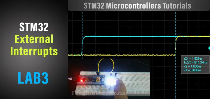
Every GPIO pin on the Nucleo-F411RE can be an external interrupt source. The STM32F411RE has 16 EXTI lines for the pins, one per pin number, so PA0, PB0 and PC0 all share EXTI0 and only one of them can use it at a time.
| EXTI Line | Pins That Can Use It | Interrupt Vector |
|---|---|---|
| EXTI0 – EXTI4 | Px0 – Px4 (one port each) | EXTI0_IRQn … EXTI4_IRQn (one each) |
| EXTI5 – EXTI9 | Px5 – Px9 | EXTI9_5_IRQn (shared) |
| EXTI10 – EXTI15 | Px10 – Px15 (B1 = PC13 on EXTI13) | EXTI15_10_IRQn (shared) |
The user button B1 on PC13 is the easiest pin to try an interrupt with: it has an external pull-up and reads LOW when pressed, so set a falling-edge trigger. In Arduino, attachInterrupt(digitalPinToInterrupt(pin), isr, FALLING) works on any pin.
Note: PC13 is not a wake-up pin on the F411 (the only WKUP pin is PA0, A0), so B1 can’t wake the MCU from Standby. Use its EXTI interrupt to wake it from Stop mode instead, or wire your wake-up signal to A0 (at 3.3v, since A0 is not 5v tolerant).
Learn more in our STM32 External Interrupt Tutorial.
Also Read
Nucleo-F411RE ADC Pins
The Nucleo-F411RE has 1x 12-bit ADC with 16 external channels, and 9 of them are on the Arduino headers: A0–A5 plus D11, D12 and D13. The ADC reference is VDD (3.3v) by default, so the input range is 0v to 3.3v.
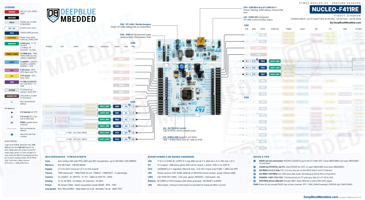
| Arduino Pin | GPIO | ADC Channel | Header Pins |
|---|---|---|---|
| A0 | PA0 | ADC1_IN0 | CN8-1, CN7-28 |
| A1 | PA1 | ADC1_IN1 | CN8-2, CN7-30 |
| A2 | PA4 | ADC1_IN4 | CN8-3, CN7-32 |
| A3 | PB0 | ADC1_IN8 | CN8-4, CN7-34 |
| A4 | PC1 | ADC1_IN11 | CN8-5, CN7-36 |
| A5 | PC0 | ADC1_IN10 | CN8-6, CN7-38 |
| D11 | PA7 | ADC1_IN7 | CN5-4, CN10-15 |
| D12 | PA6 | ADC1_IN6 | CN5-5, CN10-13 |
| D13 | PA5 | ADC1_IN5 | CN5-6, CN10-11 |
| – | PB1 | ADC1_IN9 | CN10-24 |
| – | PC2 | ADC1_IN12 | CN7-35 |
| – | PC3 | ADC1_IN13 | CN7-37 |
| – | PC4 | ADC1_IN14 | CN10-34 |
| – | PC5 | ADC1_IN15 | CN10-6 |
The ADC runs at up to 2.4Msps, and all 16 channels share that one ADC, so scanning several channels divides the sample rate between them. PA2 and PA3 (ADC1_IN2/IN3) are also analog pins, but they’re taken by the Virtual COM port.
Note: A pin in analog mode is never 5v tolerant, so keep every ADC input between 0v and 3.3v. Use a voltage divider to measure higher voltages. A0 (PA0) is 3.3v-only even as a digital pin.
There are so many sensors that we can read with the ADC pins, which include: potentiometers, LDRs, analog temperature sensors (LM35, NTC thermistors), current sensors (ACS712), joysticks, soil moisture sensors, and much more.
Learn more in our STM32 ADC Tutorial series.
Also Read
Nucleo-F411RE PWM Pins
The Nucleo-F411RE has 17 PWM pins on the Arduino headers (D2–D15, A0, A1 and A3) and 27 in total across the Morpho headers. The PWM pins are highlighted in orange in the pinout diagrams.
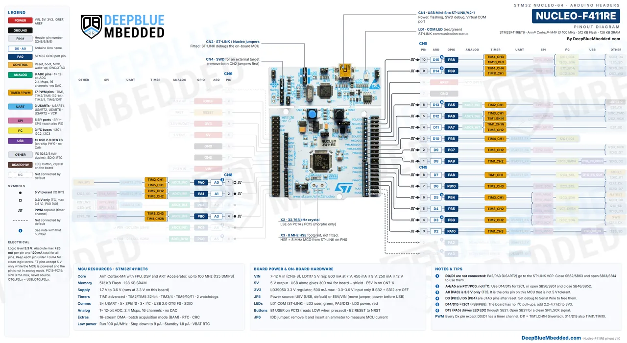
| Arduino Pin | GPIO | Timer Channel | Arduino Pin | GPIO | Timer Channel |
|---|---|---|---|---|---|
| D2 | PA10 | TIM1_CH3 | D10 | PB6 | TIM4_CH1 |
| D3 | PB3 | TIM2_CH2 | D11 | PA7 | TIM1_CH1N (or TIM3_CH2) |
| D4 | PB5 | TIM3_CH2 | D12 | PA6 | TIM3_CH1 |
| D5 | PB4 | TIM3_CH1 | D13 | PA5 | TIM2_CH1 |
| D6 | PB10 | TIM2_CH3 | D14 | PB9 | TIM4_CH4 (or TIM11_CH1) |
| D7 | PA8 | TIM1_CH1 | D15 | PB8 | TIM4_CH3 (or TIM10_CH1) |
| D8 | PA9 | TIM1_CH2 | A0 | PA0 | TIM2_CH1 / TIM5_CH1 |
| D9 | PC7 | TIM3_CH2 | A1 | PA1 | TIM2_CH2 / TIM5_CH2 |
| A3 | PB0 | TIM3_CH3 (or TIM1_CH2N) |
Nucleo-F411RE D11 PWM: The Complementary Channel
D11 (PA7) is TIM1_CH1N in UM1724, a complementary output. It’s the inverted twin of TIM1_CH1 (D7), meant for half-bridge and motor-control drivers. With HAL, start it with HAL_TIMEx_PWMN_Start(&htim1, TIM_CHANNEL_1), not HAL_TIM_PWM_Start, and remember that TIM1 is an advanced timer, so its outputs only switch on once the main output (MOE) is enabled. If you just want a plain PWM on D11, use its other channel, TIM3_CH2.
Pins on the same timer share its frequency, and some pins share the same channel: D4, D9 and D11 can all be TIM3_CH2, D5 and D12 are both TIM3_CH1, D13 and A0 can both be TIM2_CH1, and D3 and A1 can both be TIM2_CH2. Two pins on one channel always output the same duty cycle, so pick another timer (A0/A1 can use TIM5) when you need them separately. TIM2 and TIM5 are 32-bit timers; the rest are 16-bit.
There are so many things that we can control with PWM, which include: LED dimming, DC motor speed (with a driver), servo motors, buzzers, ESCs for brushless motors, and much more.
Calculate your timer settings with this STM32 PWM Calculator.
Learn more in our STM32 PWM Tutorial series.

Also Read
Nucleo-F411RE UART Pins
The Nucleo-F411RE has 3 USARTs: USART1, USART2 and USART6. USART2 (PA2/PA3) is wired to the ST-LINK Virtual COM port, so it reaches your PC through the USB cable, not the D0/D1 pins.
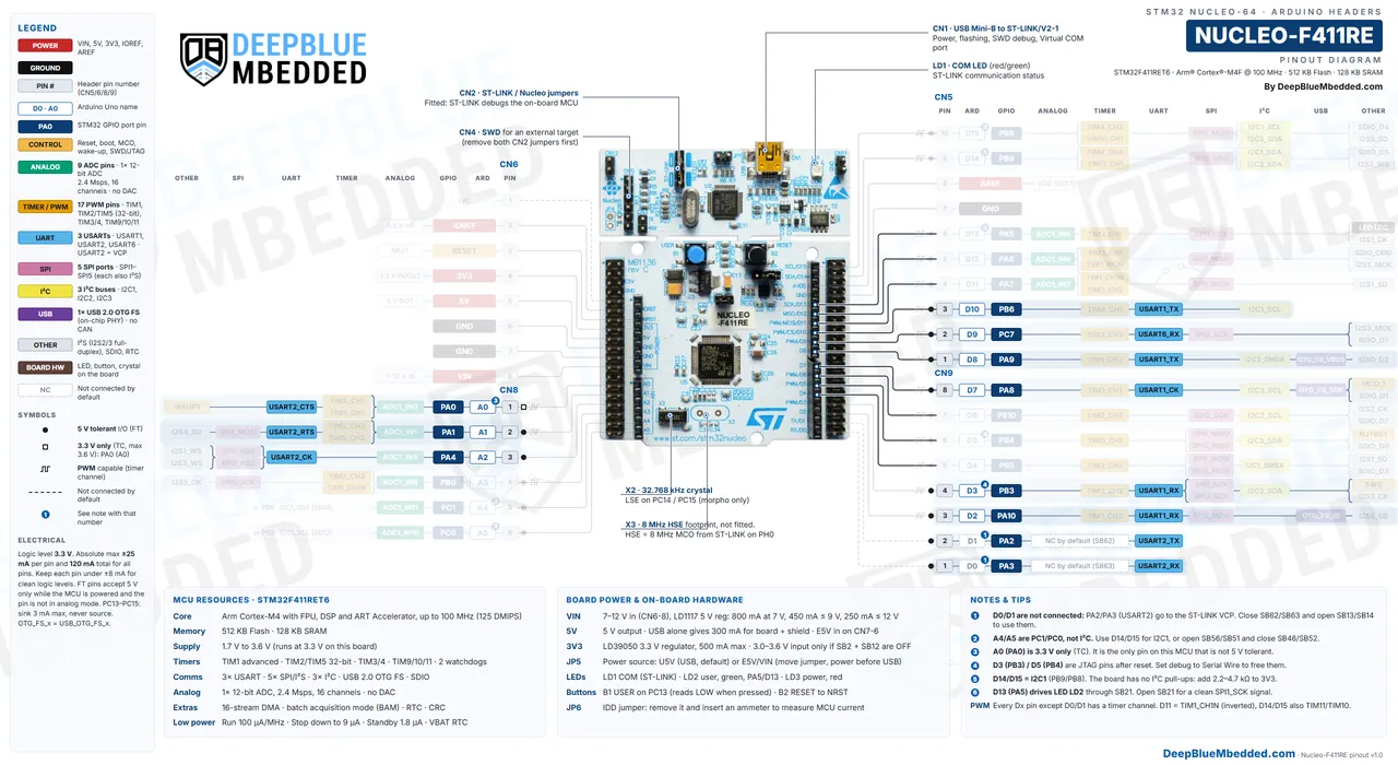
Nucleo-F411RE Default Serial (USART2): PA2 (TX) and PA3 (RX), to the PC over USB.
| UART | TX Pins | RX Pins | Note |
|---|---|---|---|
| USART1 | D8 (PA9), D10 (PB6), PA15 (CN7-17) | D2 (PA10), D3 (PB3), PB7 (CN7-21) | Best choice for a header UART |
| USART2 | PA2 (D1 after SB62) | PA3 (D0 after SB63) | ST-LINK Virtual COM port |
| USART6 | PC6 (CN10-4), PA11 (CN10-14) | D9 (PC7), PA12 (CN10-12) | PA11/PA12 are also the USB pins |
Why Doesn’t Serial Work on Nucleo-F411RE D0/D1?
Because D0 and D1 are not connected by default. On the Nucleo-F411RE, USART2 (PA2/PA3) goes to the ST-LINK through SB13/SB14, and SB62/SB63, which would connect it to D1/D0, are open. So Serial already talks to your PC over USB, and a shield that uses D0/D1 for serial gets nothing.
- Easiest fix: move the module to USART1 on D8 (TX) and D2 (RX). In Arduino: HardwareSerial Serial1(PA10, PA9); (RX first, then TX).
- If the shield must use D0/D1: open SB13/SB14 and close SB62/SB63. You lose the USB Virtual COM port when you do this.
Note: D0/D1 also have PWM (TIM2/TIM5/TIM9 channels on PA3/PA2), but they can’t reach the header either, and users report the same “PWM on PA_2 does nothing” surprise (Mbed Q&A). The fix is the same: use another pin, or move the solder bridges.
There are so many modules that we can interface with the UART pins, which include: GPS modules, Bluetooth modules (HC-05), ESP8266/ESP32 Wi-Fi modules, GSM modules, RS485 transceivers, fingerprint sensors, and much more.
Learn more in our STM32 UART Tutorial series.
Also Read
Nucleo-F411RE I2C Pins
The Nucleo-F411RE has 3x I2C buses. The default I2C1 pins are D15 (PB8, SCL) and D14 (PB9, SDA), which are the Arduino Uno R3 SCL/SDA pins next to AREF.
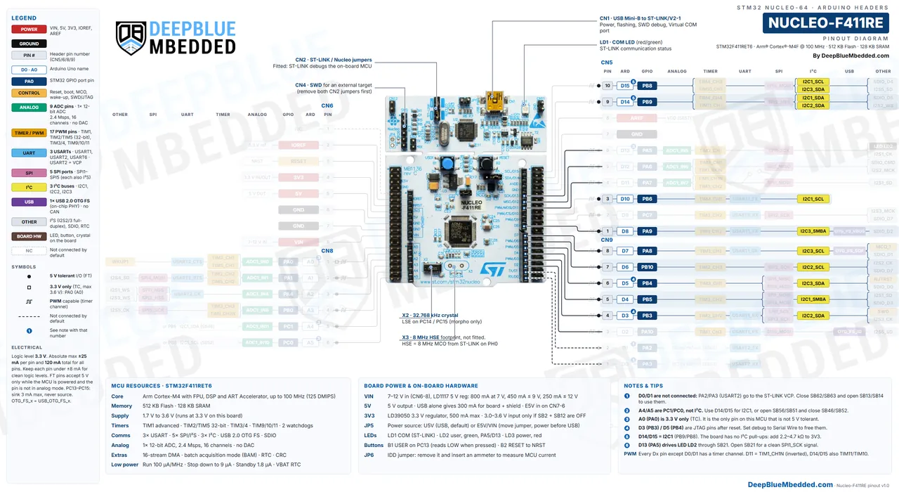
Nucleo-F411RE Default I2C1 Pins: D14 = PB9 (SDA) and D15 = PB8 (SCL).
| I2C Bus | SCL Pins | SDA Pins | Note |
|---|---|---|---|
| I2C1 | D15 (PB8), D10 (PB6) | D14 (PB9), PB7 (CN7-21) | Default Wire bus |
| I2C2 | D6 (PB10) | D3 (PB3), D14 (PB9) | PB3 is SWO after reset |
| I2C3 | D7 (PA8) | D5 (PB4), D15 (PB8), PC9 (CN10-1) | PB4 is NJTRST after reset |
Are Nucleo-F411RE A4/A5 I2C Pins?
No, not by default. On the Nucleo-F411RE, A4 and A5 are PC1 and PC0, which are ADC inputs with no I2C function. Uno shields that expect I2C on A4/A5 need either jumper wires to D14/D15, or a solder-bridge change: open SB51/SB56 and close SB46/SB52 to put I2C1 PB9 (SDA) and PB8 (SCL) on A4/A5. (Some pin maps online say PB7/PB6 here; the MB1136 schematic routes PB9/PB8.)
Note: There are no I2C pull-up resistors on the board, so add 4.7kΩ pull-ups to 3.3v unless your module already has them. Also, D15/PB8 and D10/PB6 are both I2C1_SCL, so only one of them can be the clock at a time.
When an I2C sensor doesn’t answer, check the wiring against this table first. Users report “no I2C communication” threads on this board that came down to the module being on the wrong header pins (ST Community).
There are so many modules and sensors that we can interface with the I2C bus, which include: OLED displays (SSD1306), I2C LCDs, RTC modules (DS3231), IMUs (MPU6050), BME280 sensors, EEPROMs, and much more.
Learn more in our STM32 I2C Tutorial series.
Also Read
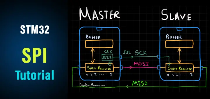
Nucleo-F411RE SPI Pins
The Nucleo-F411RE has 5x SPI ports (SPI1 to SPI5), and each one also works as I²S. The default SPI1 pins are D13 (SCK), D12 (MISO) and D11 (MOSI), just like on an Arduino Uno.
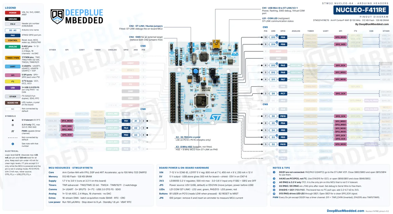
Nucleo-F411RE Default SPI1 Pins: D13 = PA5 (SCK), D12 = PA6 (MISO), D11 = PA7 (MOSI), and any GPIO (usually D10) as CS.
| SPI Port | SCK | MISO | MOSI | NSS |
|---|---|---|---|---|
| SPI1 | D13 (PA5), D3 (PB3) | D12 (PA6), D5 (PB4) | D11 (PA7), D4 (PB5) | A2 (PA4), PA15 |
| SPI2 | D6 (PB10), D9 (PC7), PB13 | PB14, PC2 | PB15, PC3 | PB12, D14 (PB9) |
| SPI3 | D3 (PB3), PC10, PB12 | D5 (PB4), PC11 | D4 (PB5), PC12 | A2 (PA4), PA15 |
| SPI4 | PB13 (CN10-30) | PA11 (CN10-14) | A1 (PA1) | PB12 (CN10-16) |
| SPI5 | A3 (PB0) | PA12 (CN10-12) | D2 (PA10), D15 (PB8) | PB1 (CN10-24) |
SPI4 and SPI5 are new on the F411 compared with the F401. They share pins with other jobs, though: SPI4_MISO and SPI5_MISO sit on the USB data pins PA11/PA12, so you can’t use them together with USB.
Note: D13 (SPI1_SCK) also drives the green LED LD2, so the LED flickers during SPI transfers. That’s normal. For the cleanest clock, use SPI1 or SPI3 on D3/D5/D4 instead, after setting the debug port to Serial Wire.
There are so many modules that we can interface with the SPI bus, which include: TFT displays (ILI9341, ST7735), SD card modules, nRF24L01 radios, MAX7219 LED drivers, W5500 Ethernet modules, and much more.
Learn more in our STM32 SPI Tutorial series.
Also Read
Nucleo-F411RE USB Pins
The STM32F411RE has 1x USB 2.0 OTG FS controller with an on-chip PHY, but the Nucleo-F411RE’s Mini-B connector only goes to the ST-LINK. To use the MCU’s own USB (CDC, HID, mass storage), wire a USB connector to PA11 (D−) and PA12 (D+) on CN10, plus GND.
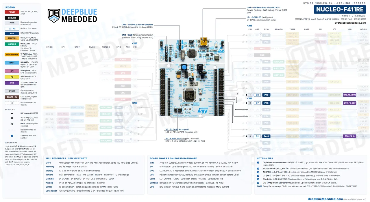
| Signal | GPIO | Header Pin | Needed? |
|---|---|---|---|
| D− (DM) | PA11 | CN10-14 | Yes |
| D+ (DP) | PA12 | CN10-12 | Yes |
| VBUS sense | PA9 | D8, CN10-21 | Optional (disable VBUS sensing in CubeMX if not wired) |
| ID | PA10 | D2, CN10-33 | Only for OTG host/device role detection |
| SOF | PA8 | D7, CN10-23 | No |
Why Does Nucleo-F411RE USB Need 96MHz Instead of 100MHz?
Because USB needs exactly 48MHz, and the PLL can’t make 100MHz and 48MHz at the same time. The F411’s USB clock is the PLL’s VCO divided by PLLQ (an integer), so with the VCO set for a 100MHz system clock you get 50MHz or 44.4MHz on USB, and the device won’t enumerate. Run the Nucleo-F411RE at 96MHz instead:
| Setting | Value (from the 8MHz HSE bypass clock) |
|---|---|
| PLLM | 4 (2MHz into the PLL) |
| PLLN | 192 (384MHz VCO) |
| PLLP | 4 (96MHz SYSCLK) |
| PLLQ | 8 (48MHz USB clock) |
| Flash latency | 3 wait states at 3.3v |
| APB1 prescaler | /2 (48MHz, the limit is 50MHz) |
You lose only 4% of the speed. Users who kept 100MHz report exactly this problem (Mbed Q&A: USB clock is 44.4MHz). The same applies to the STM32duino Arduino core: its default clock for this board is 100MHz with PLLQ = 4, which gives the USB peripheral 50MHz, so for USB CDC override the weak SystemClock_Config() with the 96MHz settings above.
Note: D7, D8 and D2 carry only the SOF, VBUS and ID signals of USB OTG. The data lines PA11/PA12 are not on the Arduino headers, so a “USB on the Arduino pins” setup isn’t possible on this board. The 16MHz HSI isn’t accurate enough for USB either, so keep the 8MHz HSE bypass clock from the ST-LINK.
Learn more in our STM32 USB CDC Tutorial.
Also Read
Nucleo-F411RE Debug (SWD) & Boot Pins
The Nucleo-F411RE is programmed and debugged over SWD on PA13 (SWDIO) and PA14 (SWCLK), with PB3 (SWO) for trace output, all wired to the on-board ST-LINK/V2-1. The boot mode is set by BOOT0 (CN7-7) and PB2/BOOT1 (CN10-22).
| Pin | Header Pin | Function After Reset |
|---|---|---|
| PA13 | CN7-13 | SWDIO (JTMS) |
| PA14 | CN7-15 | SWCLK (JTCK) |
| PB3 | D3, CN10-31 | SWO (JTDO), to the ST-LINK via SB15 |
| PA15 | CN7-17 | JTDI |
| PB4 | D5, CN10-27 | NJTRST |
| NRST | CN6-3, CN7-14 | Reset (B2 button, ST-LINK) |
| BOOT0 | CN7-7 | Pulled LOW by 10kΩ |
| PB2 (BOOT1) | CN10-22 | Read at reset when BOOT0 = 1 |
| BOOT0 | BOOT1 (PB2) | Boots From |
|---|---|---|
| 0 | any | Main Flash (normal) |
| 1 | 0 | System memory (ST bootloader) |
| 1 | 1 | Embedded SRAM |
Nucleo-F411RE Bootloader Pins (AN2606)
To start the ST system bootloader, place a jumper from CN7-5 (VDD) to CN7-7 (BOOT0) and reset the board. According to AN2606 Rev 71 (section 38, Table 84), the STM32F411xx bootloader (V13.0) listens on these pins:
| Interface | Pins | On the Nucleo-F411RE |
|---|---|---|
| USART1 | PA9 (TX), PA10 (RX) | D8 / D2: use a USB-to-serial adapter, 8 bits, even parity |
| USART2 | PD5 (TX), PD6 (RX) | Not available: the 64-pin chip has no PD5/PD6 |
| I2C1 | PB6 (SCL), PB7 (SDA) | D10 / CN7-21 |
| I2C2 | PB10 (SCL), PB3 (SDA) | D6 / D3 |
| I2C3 | PA8 (SCL), PB4 (SDA) | D7 / D5 |
| SPI1 | PA5 (SCK), PA6 (MISO), PA7 (MOSI), PA4 (NSS) | D13 / D12 / D11 / A2 |
| SPI2 | PB13, PB14, PB15, PB12 | CN10-30 / 28 / 26 / 16 |
| SPI3 | PC10, PC11, PC12, PA15 | CN7-1 / 2 / 3 / 17 |
| USB DFU | PA11 (DM), PA12 (DP) | CN10-14 / 12, needs an external clock (4MHz–26MHz, multiple of 1MHz) |
Note: The F411’s USART2 bootloader uses PD5/PD6, not PA2/PA3, so the system bootloader can’t be reached through the ST-LINK Virtual COM port on this board. Use USART1 on D8/D2 with an adapter, or simply flash with the on-board ST-LINK.
To debug another STM32 board with the on-board ST-LINK, remove both CN2 jumpers and use the 6-pin CN4 SWD connector (1 VDD_TARGET, 2 SWCLK, 3 GND, 4 SWDIO, 5 NRST, 6 SWO).
Learn more in our STM32 SWD Debugging Tutorial.
Also Read
Nucleo-F411RE On-Board Features
Besides the headers, the Nucleo-F411RE has 3 LEDs, 2 buttons, a few jumpers, and a long list of solder bridges. Here’s what each one does.
| Part | Pin / Connection | What It Does |
|---|---|---|
| LD1 COM (red/green) | ST-LINK | Red blinking: before USB init. Red: ready. Green: target connected. Red/green blinking: communicating. Orange: communication failure |
| LD2 USER (green) | PA5 / D13 (SB21) | HIGH = on |
| LD3 PWR (red) | +5V | The board is powered (off on USB if the PC refused the 300mA) |
| B1 USER (blue) | PC13 (SB17) | External pull-up, reads LOW when pressed |
| B2 RESET (black) | NRST | Resets the MCU |
| JP1 | U5V | ON: limits the USB request to 100mA, lets a USB charger power the board |
| JP5 | Power select | U5V (default) or E5V (for VIN and E5V) |
| JP6 (IDD) | MCU supply | Remove it and insert an ammeter to measure the MCU current |
| CN2 | ST-LINK jumpers | ON: the ST-LINK debugs the on-board MCU. OFF: use CN4 for an external target |
Nucleo-F411RE Solder Bridges
These are the solder bridges you’re most likely to change (UM1724 Table 10, defaults checked against the MB1136 schematic):
| Bridge | Default | Effect |
|---|---|---|
| SB13, SB14 | ON | PA2/PA3 (USART2) to the ST-LINK Virtual COM port |
| SB62, SB63 | OFF | PA2/PA3 not on D1/D0 (close them to use D0/D1) |
| SB51, SB56 | ON | A5 = PC0, A4 = PC1 |
| SB46, SB52 | OFF | Close (and open SB51/SB56) to put I2C1 PB9/PB8 on A4/A5 |
| SB21 | ON | LED LD2 on PA5 |
| SB16, SB50 | ON | 8MHz MCO from the ST-LINK into PH0 |
| SB55 | OFF | PH0 not on CN7-29 |
| SB48, SB49 | OFF | PC14/PC15 go to X2, not to CN7-25/27 |
| SB45 | ON | VBAT = VDD |
| SB57 | ON | AVDD/AREF = VDD |
| SB2, SB12 | ON | 3.3v regulator output, ST-LINK NRST |
| SB15 | ON | SWO (PB3) to the ST-LINK |
| SB17 | ON | B1 button on PC13 |
Getting Started With Nucleo-F411RE
You can program the Nucleo-F411RE with any of the common STM32 toolchains, and the ST-LINK on board means you don’t need anything else besides a Mini-USB cable.
- STM32CubeIDE: start a new project from the Board Selector, pick NUCLEO-F411RE, and let CubeMX set up the clock, LD2, B1 and USART2 for you. Set HSE to “BYPASS Clock Source” for the 8MHz MCO.
- Arduino IDE (STM32duino): install “STM32 MCU based boards”, then choose Board: “Nucleo-64” and Board part number: “Nucleo F411RE”. It runs the chip at 100MHz from the HSE bypass clock.
- PlatformIO: board ID nucleo_f411re, with the STM32Cube, Arduino, Mbed or Zephyr framework.
- Zephyr RTOS: board name nucleo_f411re. Note that its board file runs the PLL at 84MHz, not 100MHz (Zephyr docs).
- Drag-and-drop: the board shows up as a USB drive called NODE_F411RE; copy a .bin file onto it to flash it.
| Arduino Name | Pin | Default |
|---|---|---|
Serial | PA2 / PA3 (USART2) | To the PC through the ST-LINK |
Wire | PB9 (SDA, D14), PB8 (SCL, D15) | I2C1 |
SPI | D13 / D12 / D11, CS on D10 | SPI1 |
LED_BUILTIN | PA5 (D13) | LD2 |
USER_BTN | PC13 | B1 |
Here’s the classic first test, blinking LD2 and printing to the Serial Monitor at 115200 baud:
|
1 2 3 4 5 6 7 8 9 10 11 |
void setup() { pinMode(LED_BUILTIN, OUTPUT); // LD2 on PA5 (D13) pinMode(USER_BTN, INPUT); // B1 on PC13, LOW when pressed Serial.begin(115200); // USART2 to the ST-LINK VCP } void loop() { digitalWrite(LED_BUILTIN, !digitalRead(LED_BUILTIN)); Serial.println(digitalRead(USER_BTN) ? "B1 released" : "B1 pressed"); delay(500); } |
With STM32CubeIDE and HAL, the same blink is HAL_GPIO_TogglePin(GPIOA, GPIO_PIN_5); in the main loop. Follow the STM32 LED Blink Code Example for the full walk-through, and set up the 100MHz clock with the STM32 RCC Clock Configuration Guide (PLL from HSE bypass or HSI, APB1 at 50MHz max, 3 Flash wait states).
Nucleo-F411RE Common Problems & Fixes
Why doesn’t Serial work on D0/D1? PA2/PA3 go to the ST-LINK Virtual COM port, and D0/D1 are disconnected by default (SB62/SB63 open). Read Serial in the PC’s terminal over USB, or use USART1 on D8/D2 for a header UART (ST mbed wiki).
Why doesn’t my I2C shield respond on A4/A5? A4/A5 are PC1/PC0, not I2C pins. Wire the module to D14 (SDA) and D15 (SCL) with 4.7kΩ pull-ups, or move SB46/SB52 and SB51/SB56 (Mbed Q&A).
Why doesn’t my USB device enumerate at 100MHz? The USB clock must be exactly 48MHz, and a 100MHz system clock gives 50MHz or 44.4MHz. Run the F411 at 96MHz (PLLM 4, PLLN 192, PLLP 4, PLLQ 8).
Why is there no PWM on D11? D11 (PA7) is TIM1_CH1N, a complementary output. Start it with HAL_TIMEx_PWMN_Start, or configure TIM3_CH2 on PA7 instead.
Why does my code hang in SystemClock_Config (HSE never ready)? There’s no HSE crystal. HSE is an 8MHz external clock from the ST-LINK, so set HSE to “BYPASS Clock Source”, not “Crystal/Ceramic Resonator”, or run from the 16MHz HSI.
Why doesn’t LD2 light up? LD2 is on PA5 (D13), not PC13 or “PD13”. Set PA5 as an output and drive it HIGH (ST Community).
Why don’t PB3 (D3) and PB4 (D5) toggle? They’re JTAG pins after reset. In CubeMX, set System Core → SYS → Debug to “Serial Wire”, which frees PB3, PB4 and PA15.
Why can’t I use PC14/PC15 as outputs? They’re wired to the 32.768kHz crystal X2 (SB48/SB49 open), and even when you reroute them they can only sink 3mA at up to 2MHz (Mbed Q&A).
Can I connect a 5v signal to A0? No. PA0 is the only pin on the STM32F411RE that isn’t 5v tolerant. Use a voltage divider, or move the signal to any other digital pin.
Why isn’t the board powered from a USB charger? A charger never enumerates, so the ST-LINK never switches 5v to the MCU and LD3 stays off. Fit jumper JP1.
Why doesn’t the bootloader answer over the Virtual COM port? The F411’s USART2 bootloader is on PD5/PD6, which this chip doesn’t have. Use USART1 on D8/D2, or the ST-LINK.
Nucleo-F411RE vs Nucleo-F401RE vs Nucleo-F446RE
The Nucleo-F411RE, Nucleo-F401RE and Nucleo-F446RE share the same MB1136 PCB, so the headers, power, LEDs and ST-LINK are identical. Only the MCU changes:
| Feature | Nucleo-F411RE | Nucleo-F401RE | Nucleo-F446RE |
|---|---|---|---|
| MCU clock | 100MHz | 84MHz | 180MHz |
| Flash / RAM | 512KB / 128KB | 512KB / 96KB | 512KB / 128KB |
| ADC | 1x 12-bit | 1x 12-bit | 3x 12-bit |
| DAC | No | No | 2 channels |
| CAN | No | No | 2x CAN 2.0B |
| UARTs | 3 | 3 | 6 |
| SPI / I2C | 5 / 3 | 3 / 3 | 3 / 3 + FMPI2C |
| USB | OTG FS | OTG FS | OTG FS + OTG HS |
| 3.3v-only pins | A0 (PA0) | None | A2 (PA4), D13 (PA5) |
Pick the Nucleo-F411RE when you want more speed and RAM than the Nucleo-F401RE, five SPI ports, or lower run current. The Nucleo-F401RE is the one where every pin is 5v tolerant, and the Nucleo-F446RE is the pick when you need CAN, a DAC, more UARTs, or 180MHz for DSP and motor control. Code moves between the three with few changes, because the board and pinout are the same.
Nucleo-F411RE Pin Details
Here is every Nucleo-F411RE header pin in physical order, with its main functions, all its alternate functions, its 5v tolerance, and a short description. The Arduino headers come first, then the two ST Morpho headers.
Nucleo-F411RE Arduino Header Pins (CN5, CN6, CN8, CN9)
Click to expand the full pin table (32 pins)
| Pin | Label | GPIO | Main Functions | All Alternate Functions | 5v Tolerant | Description |
|---|---|---|---|---|---|---|
| CN6-1 | NC | – | – | – | – | Not connected. |
| CN6-2 | IOREF | – | 3.3v ref | – | – | 3.3v I/O reference for shields. |
| CN6-3 | RESET | – | NRST | – | – | NRST: pull it LOW to reset the MCU. |
| CN6-4 | 3V3 | – | 3.3v in/out | – | – | 3.3v output from the LD39050 regulator (500mA), or 3.3v input with SB2/SB12 open. |
| CN6-5 | 5V | – | 5v out | – | – | 5v output from USB, VIN or E5V. |
| CN6-6 | GND | – | – | – | – | Ground. |
| CN6-7 | GND | – | – | – | – | Ground. |
| CN6-8 | VIN | – | 7v–12v in | – | – | 7v–12v input to the 5v regulator. |
| CN8-1 | A0 | PA0 | ADC1_IN0, TIM2_CH1, TIM5_CH1, USART2_CTS, WKUP1 | TIM2_CH1, TIM2_ETR, TIM5_CH1, USART2_CTS, ADC1_IN0, SYS_WKUP | No (3.3v only) | A0 analog input (ADC1_IN0) and the WKUP pin; also TIM2/TIM5 channel 1 PWM. The only pin on the STM32F411RE that is NOT 5v tolerant (TC, 3.3v only). |
| CN8-2 | A1 | PA1 | ADC1_IN1, TIM2_CH2, TIM5_CH2, USART2_RTS, SPI4_MOSI, I2S4_SD | TIM2_CH2, TIM5_CH2, I2S4_SD, SPI4_MOSI, USART2_RTS, ADC1_IN1 | Yes | A1 analog input (ADC1_IN1); also TIM2/TIM5 channel 2 PWM and SPI4_MOSI. |
| CN8-3 | A2 | PA4 | ADC1_IN4, USART2_CK, SPI1_NSS, SPI3_NSS, I2S1_WS, I2S3_WS | I2S1_WS, SPI1_NSS, I2S3_WS, SPI3_NSS, USART2_CK, ADC1_IN4 | Yes | A2 analog input (ADC1_IN4) and the SPI1/SPI3 NSS pin. |
| CN8-4 | A3 | PB0 | ADC1_IN8, TIM3_CH3, TIM1_CH2N, SPI5_SCK, I2S5_CK | TIM1_CH2N, TIM3_CH3, I2S5_CK, SPI5_SCK, ADC1_IN8 | Yes | A3 analog input (ADC1_IN8), TIM3_CH3 PWM and SPI5_SCK. |
| CN8-5 | A4 | PC1 | ADC1_IN11 | ADC1_IN11 | Yes | A4 analog input (ADC1_IN11); I2C1_SDA only after the SB56/SB46 change. |
| CN8-6 | A5 | PC0 | ADC1_IN10 | ADC1_IN10 | Yes | A5 analog input (ADC1_IN10); I2C1_SCL only after the SB51/SB52 change. |
| CN5-10 | D15 | PB8 | TIM4_CH3, TIM10_CH1, SPI5_MOSI, I2C1_SCL, I2C3_SDA, SDIO_D4, I2S5_SD | TIM4_CH3, TIM10_CH1, I2C1_SCL, I2S5_SD, SPI5_MOSI, I2C3_SDA, SDIO_D4 | Yes | D15: the default I2C1_SCL (Wire), also TIM4_CH3/TIM10_CH1 PWM, SPI5_MOSI and I2C3_SDA. |
| CN5-9 | D14 | PB9 | TIM4_CH4, TIM11_CH1, SPI2_NSS, I2C1_SDA, I2C2_SDA, SDIO_D5, I2S2_WS | TIM4_CH4, TIM11_CH1, I2C1_SDA, I2S2_WS, SPI2_NSS, I2C2_SDA, SDIO_D5 | Yes | D14: the default I2C1_SDA (Wire), also TIM4_CH4/TIM11_CH1 PWM, SPI2_NSS and I2C2_SDA. |
| CN5-8 | AREF | – | = VDD (SB57) | – | – | ADC reference, tied to VDD by SB57. |
| CN5-7 | GND | – | – | – | – | Ground. |
| CN5-6 | D13 | PA5 | ADC1_IN5, TIM2_CH1, SPI1_SCK, LED LD2, I2S1_CK | TIM2_CH1, TIM2_ETR, I2S1_CK, SPI1_SCK, ADC1_IN5 | Yes | D13: drives the green user LED LD2, SPI1_SCK, ADC1_IN5 and TIM2_CH1 PWM. |
| CN5-5 | D12 | PA6 | ADC1_IN6, TIM3_CH1, TIM1_BKIN, SPI1_MISO, SDIO_CMD, I2S2_MCK | TIM1_BKIN, TIM3_CH1, SPI1_MISO, I2S2_MCK, SDIO_CMD, ADC1_IN6 | Yes | D12: SPI1_MISO, ADC1_IN6 and TIM3_CH1 PWM. |
| CN5-4 | D11 | PA7 | ADC1_IN7, TIM1_CH1N, TIM3_CH2, SPI1_MOSI, I2S1_SD | TIM1_CH1N, TIM3_CH2, I2S1_SD, SPI1_MOSI, ADC1_IN7 | Yes | D11: SPI1_MOSI, ADC1_IN7 and PWM on TIM1_CH1N (complementary) or TIM3_CH2. |
| CN5-3 | D10 | PB6 | TIM4_CH1, USART1_TX, I2C1_SCL | TIM4_CH1, I2C1_SCL, USART1_TX | Yes | D10: USART1_TX, I2C1_SCL and TIM4_CH1 PWM. |
| CN5-2 | D9 | PC7 | TIM3_CH2, USART6_RX, SPI2_SCK, I2S3_MCK, SDIO_D7 | TIM3_CH2, I2S2_CK, SPI2_SCK, I2S3_MCK, USART6_RX, SDIO_D7 | Yes | D9: USART6_RX, SPI2_SCK and TIM3_CH2 PWM. |
| CN5-1 | D8 | PA9 | TIM1_CH2, USART1_TX, I2C3_SMBA, OTG_FS_VBUS, SDIO_D2 | TIM1_CH2, I2C3_SMBA, USART1_TX, USB_OTG_FS_VBUS, SDIO_D2 | Yes | D8: USART1_TX, TIM1_CH2 PWM and the USB OTG FS VBUS sense input. |
| CN9-8 | D7 | PA8 | TIM1_CH1, USART1_CK, I2C3_SCL, OTG_FS_SOF, MCO_1, SDIO_D1 | RCC_MCO_1, TIM1_CH1, I2C3_SCL, USART1_CK, USB_OTG_FS_SOF, SDIO_D1 | Yes | D7: TIM1_CH1 PWM, I2C3_SCL, the MCO1 clock output and USB OTG FS SOF. |
| CN9-7 | D6 | PB10 | TIM2_CH3, SPI2_SCK, I2C2_SCL, I2S2_CK, SDIO_D7 | TIM2_CH3, I2C2_SCL, I2S2_CK, SPI2_SCK, I2S3_MCK, SDIO_D7 | Yes | D6: I2C2_SCL, SPI2_SCK and TIM2_CH3 PWM. |
| CN9-6 | D5 | PB4 | TIM3_CH1, SPI1_MISO, SPI3_MISO, I2C3_SDA, NJTRST, SDIO_D0 | SYS_JTRST, TIM3_CH1, SPI1_MISO, SPI3_MISO, I2S3_ext_SD, I2C3_SDA, SDIO_D0 | Yes | D5: NJTRST after reset, then SPI1/SPI3_MISO, I2C3_SDA or TIM3_CH1. |
| CN9-5 | D4 | PB5 | TIM3_CH2, SPI1_MOSI, SPI3_MOSI, I2C1_SMBA, I2S1_SD, SDIO_D3 | TIM3_CH2, I2C1_SMBA, I2S1_SD, SPI1_MOSI, I2S3_SD, SPI3_MOSI, SDIO_D3 | Yes | D4: SPI1/SPI3_MOSI and TIM3_CH2 PWM. |
| CN9-4 | D3 | PB3 | TIM2_CH2, USART1_RX, SPI1_SCK, SPI3_SCK, I2C2_SDA, SWO, I2S3_CK | SYS_JTDO-SWO, TIM2_CH2, I2S1_CK, SPI1_SCK, I2S3_CK, SPI3_SCK, USART1_RX, I2C2_SDA | Yes | D3: SWO trace output after reset (to the ST-LINK via SB15), then SPI1/SPI3_SCK, USART1_RX, I2C2_SDA or TIM2_CH2. |
| CN9-3 | D2 | PA10 | TIM1_CH3, USART1_RX, SPI5_MOSI, OTG_FS_ID, I2S5_SD | TIM1_CH3, I2S5_SD, SPI5_MOSI, USART1_RX, USB_OTG_FS_ID | Yes | D2: USART1_RX, TIM1_CH3 PWM, SPI5_MOSI and the USB OTG FS ID pin. |
| CN9-2 | D1 | PA2 | ADC1_IN2, TIM2_CH3, TIM5_CH3, USART2_TX | TIM2_CH3, TIM5_CH3, TIM9_CH1, I2S_CKIN, USART2_TX, ADC1_IN2 | Yes | USART2_TX, wired to the ST-LINK Virtual COM port, so it is not on D1 unless you close SB62. |
| CN9-1 | D0 | PA3 | ADC1_IN3, TIM2_CH4, TIM5_CH4, USART2_RX | TIM2_CH4, TIM5_CH4, TIM9_CH2, I2S2_MCK, USART2_RX, ADC1_IN3 | Yes | USART2_RX, wired to the ST-LINK Virtual COM port, so it is not on D0 unless you close SB63. |
Nucleo-F411RE Morpho CN7 Pins
On CN7, pin 1 is at the end nearest the ST-LINK, and odd pins are on the outer column.
Click to expand the full pin table (38 pins)
| Pin | Label | GPIO | Main Functions | All Alternate Functions | 5v Tolerant | Description |
|---|---|---|---|---|---|---|
| CN7-1 | – | PC10 | SPI3_SCK, I2S3_CK, SDIO_D2 | I2S3_CK, SPI3_SCK, SDIO_D2 | Yes | Morpho only: SPI3_SCK and SDIO_D2. |
| CN7-2 | – | PC11 | SPI3_MISO, SDIO_D3, I2S3ext_SD | I2S3_ext_SD, SPI3_MISO, SDIO_D3, ADC1_EXTI11 | Yes | Morpho only: SPI3_MISO and SDIO_D3. |
| CN7-3 | – | PC12 | SPI3_MOSI, I2S3_SD, SDIO_CK | I2S3_SD, SPI3_MOSI, SDIO_CK | Yes | Morpho only: SPI3_MOSI and SDIO_CK. |
| CN7-4 | – | PD2 | TIM3_ETR, SDIO_CMD | TIM3_ETR, SDIO_CMD | Yes | Morpho only: SDIO_CMD and TIM3_ETR. |
| CN7-5 | VDD | – | 3.3v (VDD) | – | – | 3.3v MCU supply (VDD). |
| CN7-6 | E5V | – | 5v external in | – | – | External 5v input (4.75v–5.25v, 500mA) with JP5 on E5V. |
| CN7-7 | BOOT0 | – | 10kΩ to GND | – | – | BOOT0, pulled LOW by 10kΩ; tie it to VDD (CN7-5) to start the system bootloader. |
| CN7-8 | GND | – | – | – | – | Ground. |
| CN7-9 | NC | – | – | – | – | Not connected. |
| CN7-10 | NC | – | – | – | – | Not connected. |
| CN7-11 | NC | – | – | – | – | Not connected. |
| CN7-12 | IOREF | – | 3.3v ref | – | – | 3.3v I/O reference for shields. |
| CN7-13 | – | PA13 | SWDIO | SYS_JTMS-SWDIO | Yes | SWDIO, used by the on-board ST-LINK to program and debug the MCU; leave it alone. |
| CN7-14 | RESET | – | NRST | – | – | NRST: pull it LOW to reset the MCU. |
| CN7-15 | – | PA14 | SWCLK | SYS_JTCK-SWCLK | Yes | SWCLK, used by the on-board ST-LINK to program and debug the MCU; leave it alone. |
| CN7-16 | 3V3 | – | 3.3v in/out | – | – | 3.3v output from the LD39050 regulator (500mA), or 3.3v input with SB2/SB12 open. |
| CN7-17 | – | PA15 | TIM2_CH1, USART1_TX, SPI1_NSS, SPI3_NSS, JTDI, I2S1_WS | SYS_JTDI, TIM2_CH1, TIM2_ETR, I2S1_WS, SPI1_NSS, I2S3_WS, SPI3_NSS, USART1_TX, ADC1_EXTI15 | Yes | JTDI after reset, then usable as TIM2_CH1, USART1_TX or SPI1/SPI3_NSS. |
| CN7-18 | 5V | – | 5v out | – | – | 5v output from USB, VIN or E5V. |
| CN7-19 | GND | – | – | – | – | Ground. |
| CN7-20 | GND | – | – | – | – | Ground. |
| CN7-21 | – | PB7 | TIM4_CH2, USART1_RX, I2C1_SDA, SDIO_D0 | TIM4_CH2, I2C1_SDA, USART1_RX, SDIO_D0 | Yes | Morpho only: USART1_RX, I2C1_SDA and TIM4_CH2 PWM. |
| CN7-22 | GND | – | – | – | – | Ground. |
| CN7-23 | – | PC13 | B1 USER, RTC_AF1 | RTC_AF1 | Yes | The blue user button B1 (reads LOW when pressed); a weak pin on the backup domain (3mA sink max). |
| CN7-24 | VIN | – | 7v–12v in | – | – | 7v–12v input to the 5v regulator. |
| CN7-25 | – | PC14 | OSC32_IN | RCC_OSC32_IN | Yes | OSC32_IN for the 32.768kHz LSE crystal X2; not connected to the header by default. |
| CN7-26 | NC | – | – | – | – | Not connected. |
| CN7-27 | – | PC15 | OSC32_OUT | ADC1_EXTI15, RCC_OSC32_OUT | Yes | OSC32_OUT for the 32.768kHz LSE crystal X2; not connected to the header by default. |
| CN7-28 | A0 | PA0 | ADC1_IN0, TIM2_CH1, TIM5_CH1, USART2_CTS, WKUP1 | TIM2_CH1, TIM2_ETR, TIM5_CH1, USART2_CTS, ADC1_IN0, SYS_WKUP | No (3.3v only) | A0 analog input (ADC1_IN0) and the WKUP pin; also TIM2/TIM5 channel 1 PWM. The only pin on the STM32F411RE that is NOT 5v tolerant (TC, 3.3v only). |
| CN7-29 | – | PH0 | OSC_IN | RCC_OSC_IN | Yes | OSC_IN, fed with the 8MHz MCO clock from the ST-LINK; not connected to the header by default. |
| CN7-30 | A1 | PA1 | ADC1_IN1, TIM2_CH2, TIM5_CH2, USART2_RTS, SPI4_MOSI, I2S4_SD | TIM2_CH2, TIM5_CH2, I2S4_SD, SPI4_MOSI, USART2_RTS, ADC1_IN1 | Yes | A1 analog input (ADC1_IN1); also TIM2/TIM5 channel 2 PWM and SPI4_MOSI. |
| CN7-31 | – | PH1 | OSC_OUT | RCC_OSC_OUT | Yes | OSC_OUT; free on the header, but not usable as an output while HSE runs in bypass mode. |
| CN7-32 | A2 | PA4 | ADC1_IN4, USART2_CK, SPI1_NSS, SPI3_NSS, I2S1_WS, I2S3_WS | I2S1_WS, SPI1_NSS, I2S3_WS, SPI3_NSS, USART2_CK, ADC1_IN4 | Yes | A2 analog input (ADC1_IN4) and the SPI1/SPI3 NSS pin. |
| CN7-33 | VBAT | – | = VDD (SB45) | – | – | RTC/backup supply, tied to VDD by SB45. |
| CN7-34 | A3 | PB0 | ADC1_IN8, TIM3_CH3, TIM1_CH2N, SPI5_SCK, I2S5_CK | TIM1_CH2N, TIM3_CH3, I2S5_CK, SPI5_SCK, ADC1_IN8 | Yes | A3 analog input (ADC1_IN8), TIM3_CH3 PWM and SPI5_SCK. |
| CN7-35 | – | PC2 | ADC1_IN12, SPI2_MISO, I2S2ext_SD | SPI2_MISO, I2S2_ext_SD, ADC1_IN12 | Yes | Morpho only: ADC1_IN12 analog input and SPI2_MISO. |
| CN7-36 | A4 | PC1 | ADC1_IN11 | ADC1_IN11 | Yes | A4 analog input (ADC1_IN11); I2C1_SDA only after the SB56/SB46 change. |
| CN7-37 | – | PC3 | ADC1_IN13, SPI2_MOSI, I2S2_SD | I2S2_SD, SPI2_MOSI, ADC1_IN13 | Yes | Morpho only: ADC1_IN13 analog input and SPI2_MOSI. |
| CN7-38 | A5 | PC0 | ADC1_IN10 | ADC1_IN10 | Yes | A5 analog input (ADC1_IN10); I2C1_SCL only after the SB51/SB52 change. |
Nucleo-F411RE Morpho CN10 Pins
On CN10, pin 1 is also at the ST-LINK end, but odd pins are on the inner column.
Click to expand the full pin table (38 pins)
| Pin | Label | GPIO | Main Functions | All Alternate Functions | 5v Tolerant | Description |
|---|---|---|---|---|---|---|
| CN10-1 | – | PC9 | TIM3_CH4, I2C3_SDA, MCO_2, SDIO_D1 | RCC_MCO_2, TIM3_CH4, I2C3_SDA, I2S_CKIN, SDIO_D1 | Yes | Morpho only: TIM3_CH4 PWM, I2C3_SDA and the MCO2 clock output. |
| CN10-2 | – | PC8 | TIM3_CH3, USART6_CK, SDIO_D0 | TIM3_CH3, USART6_CK, SDIO_D0 | Yes | Morpho only: TIM3_CH3 PWM and SDIO_D0. |
| CN10-3 | D15 | PB8 | TIM4_CH3, TIM10_CH1, SPI5_MOSI, I2C1_SCL, I2C3_SDA, SDIO_D4, I2S5_SD | TIM4_CH3, TIM10_CH1, I2C1_SCL, I2S5_SD, SPI5_MOSI, I2C3_SDA, SDIO_D4 | Yes | D15: the default I2C1_SCL (Wire), also TIM4_CH3/TIM10_CH1 PWM, SPI5_MOSI and I2C3_SDA. |
| CN10-4 | – | PC6 | TIM3_CH1, USART6_TX, I2S2_MCK, SDIO_D6 | TIM3_CH1, I2S2_MCK, USART6_TX, SDIO_D6 | Yes | Morpho only: USART6_TX and TIM3_CH1 PWM. |
| CN10-5 | D14 | PB9 | TIM4_CH4, TIM11_CH1, SPI2_NSS, I2C1_SDA, I2C2_SDA, SDIO_D5, I2S2_WS | TIM4_CH4, TIM11_CH1, I2C1_SDA, I2S2_WS, SPI2_NSS, I2C2_SDA, SDIO_D5 | Yes | D14: the default I2C1_SDA (Wire), also TIM4_CH4/TIM11_CH1 PWM, SPI2_NSS and I2C2_SDA. |
| CN10-6 | – | PC5 | ADC1_IN15 | ADC1_IN15 | Yes | Morpho only: ADC1_IN15 analog input. |
| CN10-7 | AVDD | – | = VDD (SB57) | – | – | Analog supply VDDA, tied to VDD by SB57. |
| CN10-8 | U5V | – | USB 5v | – | – | 5v from the ST-LINK USB connector. |
| CN10-9 | GND | – | – | – | – | Ground. |
| CN10-10 | NC | – | – | – | – | Not connected. |
| CN10-11 | D13 | PA5 | ADC1_IN5, TIM2_CH1, SPI1_SCK, LED LD2, I2S1_CK | TIM2_CH1, TIM2_ETR, I2S1_CK, SPI1_SCK, ADC1_IN5 | Yes | D13: drives the green user LED LD2, SPI1_SCK, ADC1_IN5 and TIM2_CH1 PWM. |
| CN10-12 | – | PA12 | TIM1_ETR, USART1_RTS, USART6_RX, SPI5_MISO, OTG_FS_DP | TIM1_ETR, SPI5_MISO, USART1_RTS, USART6_RX, USB_OTG_FS_DP | Yes | Morpho only: USB OTG FS D+ (DP), USART6_RX, SPI5_MISO or TIM1_ETR. |
| CN10-13 | D12 | PA6 | ADC1_IN6, TIM3_CH1, TIM1_BKIN, SPI1_MISO, SDIO_CMD, I2S2_MCK | TIM1_BKIN, TIM3_CH1, SPI1_MISO, I2S2_MCK, SDIO_CMD, ADC1_IN6 | Yes | D12: SPI1_MISO, ADC1_IN6 and TIM3_CH1 PWM. |
| CN10-14 | – | PA11 | TIM1_CH4, USART1_CTS, USART6_TX, SPI4_MISO, OTG_FS_DM | TIM1_CH4, SPI4_MISO, USART1_CTS, USART6_TX, USB_OTG_FS_DM, ADC1_EXTI11 | Yes | Morpho only: USB OTG FS D− (DM), USART6_TX, SPI4_MISO or TIM1_CH4. |
| CN10-15 | D11 | PA7 | ADC1_IN7, TIM1_CH1N, TIM3_CH2, SPI1_MOSI, I2S1_SD | TIM1_CH1N, TIM3_CH2, I2S1_SD, SPI1_MOSI, ADC1_IN7 | Yes | D11: SPI1_MOSI, ADC1_IN7 and PWM on TIM1_CH1N (complementary) or TIM3_CH2. |
| CN10-16 | – | PB12 | TIM1_BKIN, SPI2_NSS, SPI4_NSS, I2C2_SMBA, I2S2_WS, I2S3_CK | TIM1_BKIN, I2C2_SMBA, I2S2_WS, SPI2_NSS, I2S4_WS, SPI4_NSS, I2S3_CK, SPI3_SCK | Yes | Morpho only: SPI2/SPI4_NSS, SPI3_SCK and TIM1_BKIN. |
| CN10-17 | D10 | PB6 | TIM4_CH1, USART1_TX, I2C1_SCL | TIM4_CH1, I2C1_SCL, USART1_TX | Yes | D10: USART1_TX, I2C1_SCL and TIM4_CH1 PWM. |
| CN10-18 | NC | – | – | – | – | Not connected. |
| CN10-19 | D9 | PC7 | TIM3_CH2, USART6_RX, SPI2_SCK, I2S3_MCK, SDIO_D7 | TIM3_CH2, I2S2_CK, SPI2_SCK, I2S3_MCK, USART6_RX, SDIO_D7 | Yes | D9: USART6_RX, SPI2_SCK and TIM3_CH2 PWM. |
| CN10-20 | GND | – | – | – | – | Ground. |
| CN10-21 | D8 | PA9 | TIM1_CH2, USART1_TX, I2C3_SMBA, OTG_FS_VBUS, SDIO_D2 | TIM1_CH2, I2C3_SMBA, USART1_TX, USB_OTG_FS_VBUS, SDIO_D2 | Yes | D8: USART1_TX, TIM1_CH2 PWM and the USB OTG FS VBUS sense input. |
| CN10-22 | – | PB2 | BOOT1 | – | Yes | BOOT1, which must be LOW for the system bootloader; otherwise a plain GPIO (no alternate function). |
| CN10-23 | D7 | PA8 | TIM1_CH1, USART1_CK, I2C3_SCL, OTG_FS_SOF, MCO_1, SDIO_D1 | RCC_MCO_1, TIM1_CH1, I2C3_SCL, USART1_CK, USB_OTG_FS_SOF, SDIO_D1 | Yes | D7: TIM1_CH1 PWM, I2C3_SCL, the MCO1 clock output and USB OTG FS SOF. |
| CN10-24 | – | PB1 | ADC1_IN9, TIM3_CH4, TIM1_CH3N, SPI5_NSS, I2S5_WS | TIM1_CH3N, TIM3_CH4, I2S5_WS, SPI5_NSS, ADC1_IN9 | Yes | Morpho only: ADC1_IN9 analog input, TIM3_CH4 PWM and SPI5_NSS. |
| CN10-25 | D6 | PB10 | TIM2_CH3, SPI2_SCK, I2C2_SCL, I2S2_CK, SDIO_D7 | TIM2_CH3, I2C2_SCL, I2S2_CK, SPI2_SCK, I2S3_MCK, SDIO_D7 | Yes | D6: I2C2_SCL, SPI2_SCK and TIM2_CH3 PWM. |
| CN10-26 | – | PB15 | TIM1_CH3N, SPI2_MOSI, I2S2_SD, RTC_REFIN | RTC_REFIN, TIM1_CH3N, I2S2_SD, SPI2_MOSI, SDIO_CK, ADC1_EXTI15 | Yes | Morpho only: SPI2_MOSI and TIM1_CH3N PWM. |
| CN10-27 | D5 | PB4 | TIM3_CH1, SPI1_MISO, SPI3_MISO, I2C3_SDA, NJTRST, SDIO_D0 | SYS_JTRST, TIM3_CH1, SPI1_MISO, SPI3_MISO, I2S3_ext_SD, I2C3_SDA, SDIO_D0 | Yes | D5: NJTRST after reset, then SPI1/SPI3_MISO, I2C3_SDA or TIM3_CH1. |
| CN10-28 | – | PB14 | TIM1_CH2N, SPI2_MISO, I2S2ext_SD, SDIO_D6 | TIM1_CH2N, SPI2_MISO, I2S2_ext_SD, SDIO_D6 | Yes | Morpho only: SPI2_MISO and TIM1_CH2N PWM. |
| CN10-29 | D4 | PB5 | TIM3_CH2, SPI1_MOSI, SPI3_MOSI, I2C1_SMBA, I2S1_SD, SDIO_D3 | TIM3_CH2, I2C1_SMBA, I2S1_SD, SPI1_MOSI, I2S3_SD, SPI3_MOSI, SDIO_D3 | Yes | D4: SPI1/SPI3_MOSI and TIM3_CH2 PWM. |
| CN10-30 | – | PB13 | TIM1_CH1N, SPI2_SCK, SPI4_SCK, I2S2_CK, I2S4_CK | TIM1_CH1N, I2S2_CK, SPI2_SCK, I2S4_CK, SPI4_SCK | Yes | Morpho only: SPI2/SPI4_SCK and TIM1_CH1N PWM. |
| CN10-31 | D3 | PB3 | TIM2_CH2, USART1_RX, SPI1_SCK, SPI3_SCK, I2C2_SDA, SWO, I2S3_CK | SYS_JTDO-SWO, TIM2_CH2, I2S1_CK, SPI1_SCK, I2S3_CK, SPI3_SCK, USART1_RX, I2C2_SDA | Yes | D3: SWO trace output after reset (to the ST-LINK via SB15), then SPI1/SPI3_SCK, USART1_RX, I2C2_SDA or TIM2_CH2. |
| CN10-32 | AGND | – | – | – | – | Analog ground. |
| CN10-33 | D2 | PA10 | TIM1_CH3, USART1_RX, SPI5_MOSI, OTG_FS_ID, I2S5_SD | TIM1_CH3, I2S5_SD, SPI5_MOSI, USART1_RX, USB_OTG_FS_ID | Yes | D2: USART1_RX, TIM1_CH3 PWM, SPI5_MOSI and the USB OTG FS ID pin. |
| CN10-34 | – | PC4 | ADC1_IN14 | ADC1_IN14 | Yes | Morpho only: ADC1_IN14 analog input. |
| CN10-35 | D1 | PA2 | USART2_TX | TIM2_CH3, TIM5_CH3, TIM9_CH1, I2S_CKIN, USART2_TX, ADC1_IN2 | Yes | USART2_TX, wired to the ST-LINK Virtual COM port, so it is not on D1 unless you close SB62. |
| CN10-36 | NC | – | – | – | – | Not connected. |
| CN10-37 | D0 | PA3 | USART2_RX | TIM2_CH4, TIM5_CH4, TIM9_CH2, I2S2_MCK, USART2_RX, ADC1_IN3 | Yes | USART2_RX, wired to the ST-LINK Virtual COM port, so it is not on D0 unless you close SB63. |
| CN10-38 | NC | – | – | – | – | Not connected. |
PB11 does not exist on the 64-pin STM32F411RE (that package pin is VCAP1), which is why CN10-18 is not connected.
Wrap Up
To conclude this guide article, the Nucleo-F411RE is a very solid entry-level development board. It gives you a 100MHz Cortex-M4F with 512KB of Flash and 128KB of RAM, 3 UARTs, 3 I2C buses, 5 SPI ports, and USB OTG, on a board that you can program out of the box. Just remember the board-level gotchas: D0/D1 are the ST-LINK’s, A4/A5 aren’t I2C, A0 is the one pin that isn’t 5v tolerant, and USB wants a 96MHz clock.
I hope you’ve found this guide helpful for your project. For more boards, check out the Pinouts, Datasheets & Schematic Diagrams Library. Follow this STM32 Series of Tutorials to learn more about programming STM32 microcontrollers.
If you’re just getting started with STM32, you need to check out the STM32 Getting Started Ultimate Guide below.
The complete beginner’s guide to STM32 microcontrollers: the toolchain, your first project, and the STM32 tutorials series step by step.
