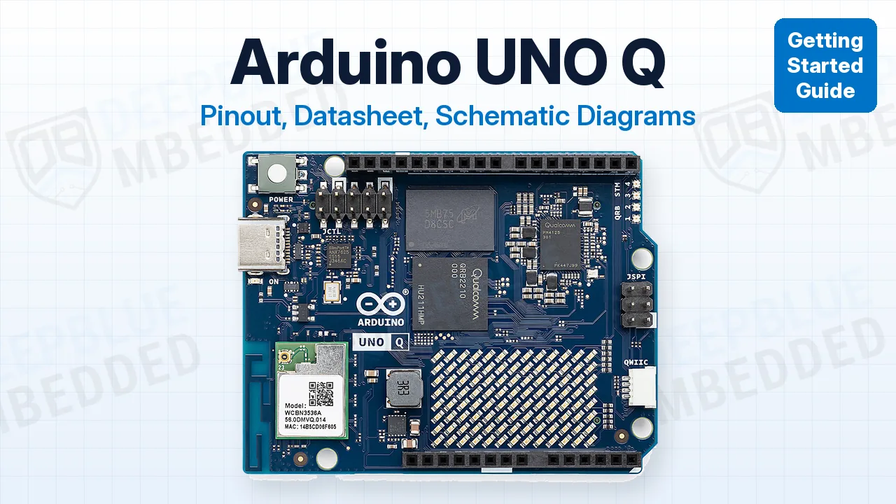
In this guide, you’ll find the Arduino UNO Q pinout diagram, its datasheet and schematic diagram, and every pin group explained with its default pins and gotchas. Without further ado, let’s get right into it!
The Arduino UNO Q is two computers on one UNO-size board: a Qualcomm Dragonwing QRB2210 (4x Cortex-A53 at 2.0GHz) running Debian Linux, and an STM32U585 microcontroller (Cortex-M33 at 160MHz) that drives the UNO headers at 3.3v logic, unlike the 5v UNO R3. It adds Wi-Fi 5, Bluetooth 5.1, an 8×13 LED matrix, and camera, display, and audio pins on the bottom side.
Arduino UNO Q Pinout Diagram
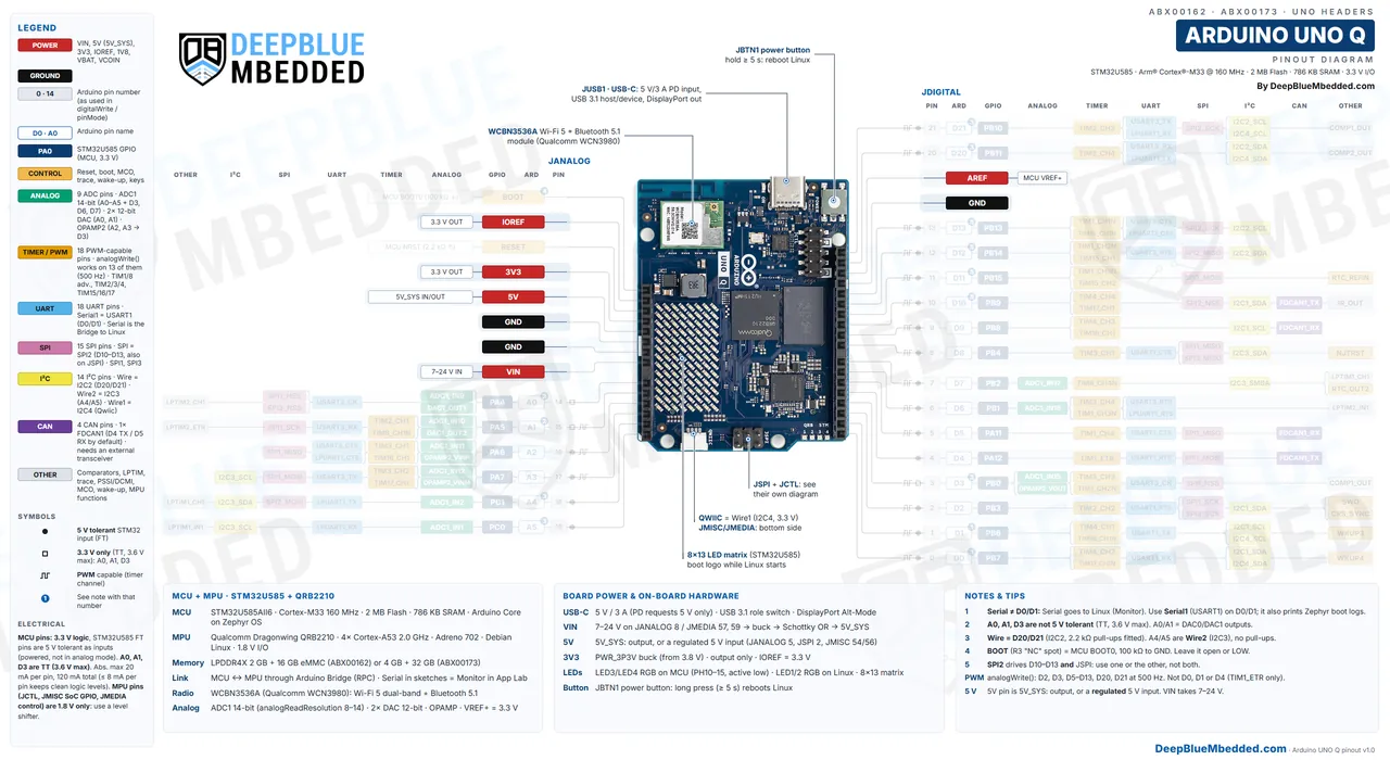
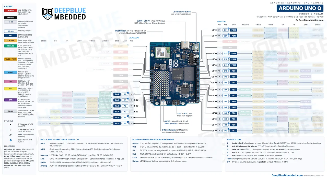
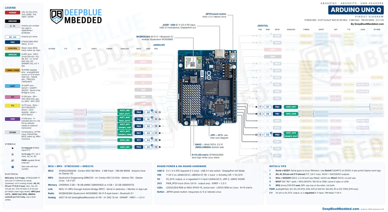
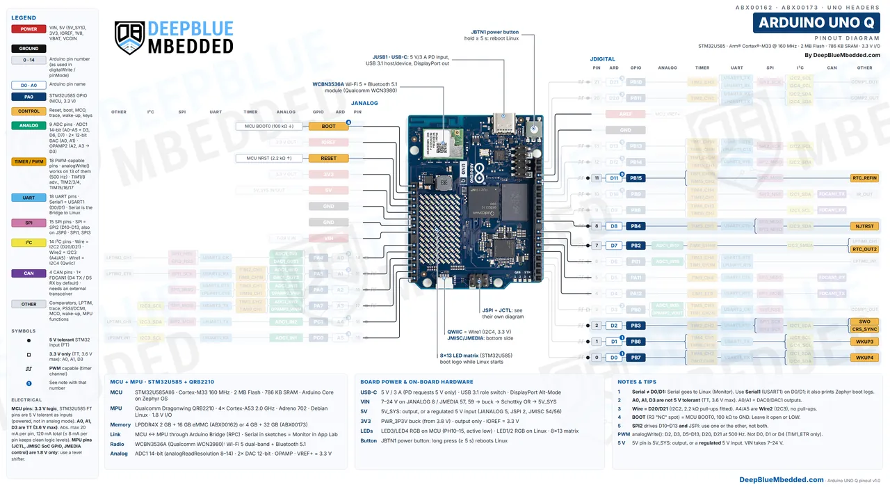
Here is a detailed Arduino UNO Q Pinout Diagram with colored labels and legends to help you easily identify the functionalities that each pin can perform. The board has seven connectors driven by two processors, so the pinout comes in four diagrams: the UNO headers first, then the small top-side headers, then the two 60-pin connectors on the bottom side.
Arduino UNO Q UNO Headers Pinout (JANALOG & JDIGITAL)
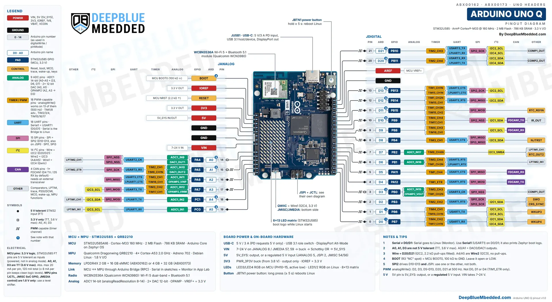
Each row shows the Arduino pin number the core uses (D0–D13 are 0–13, A0–A5 are 14–19, and the SDA/SCL pins are D20/D21), the STM32U585 GPIO (PA4, PB7…), and the pin’s functions, color-coded by peripheral. The dot symbol marks a 5v-tolerant input, the square marks a 3.3v-only pin (A0, A1, D3), and the PWM symbol marks the pins analogWrite() drives. The numbered badges point to the notes at the bottom of the diagram.
With the USB-C connector at the top, JANALOG is the left header (pin 1 = BOOT at the top, pin 14 = A5 at the bottom) and JDIGITAL is the right header (pin 1 = D0 at the bottom, pin 18 = D21/SCL at the top), the same positions as on every UNO, so UNO shields fit.
Arduino UNO Q JCTL, JSPI & Qwiic Pinout
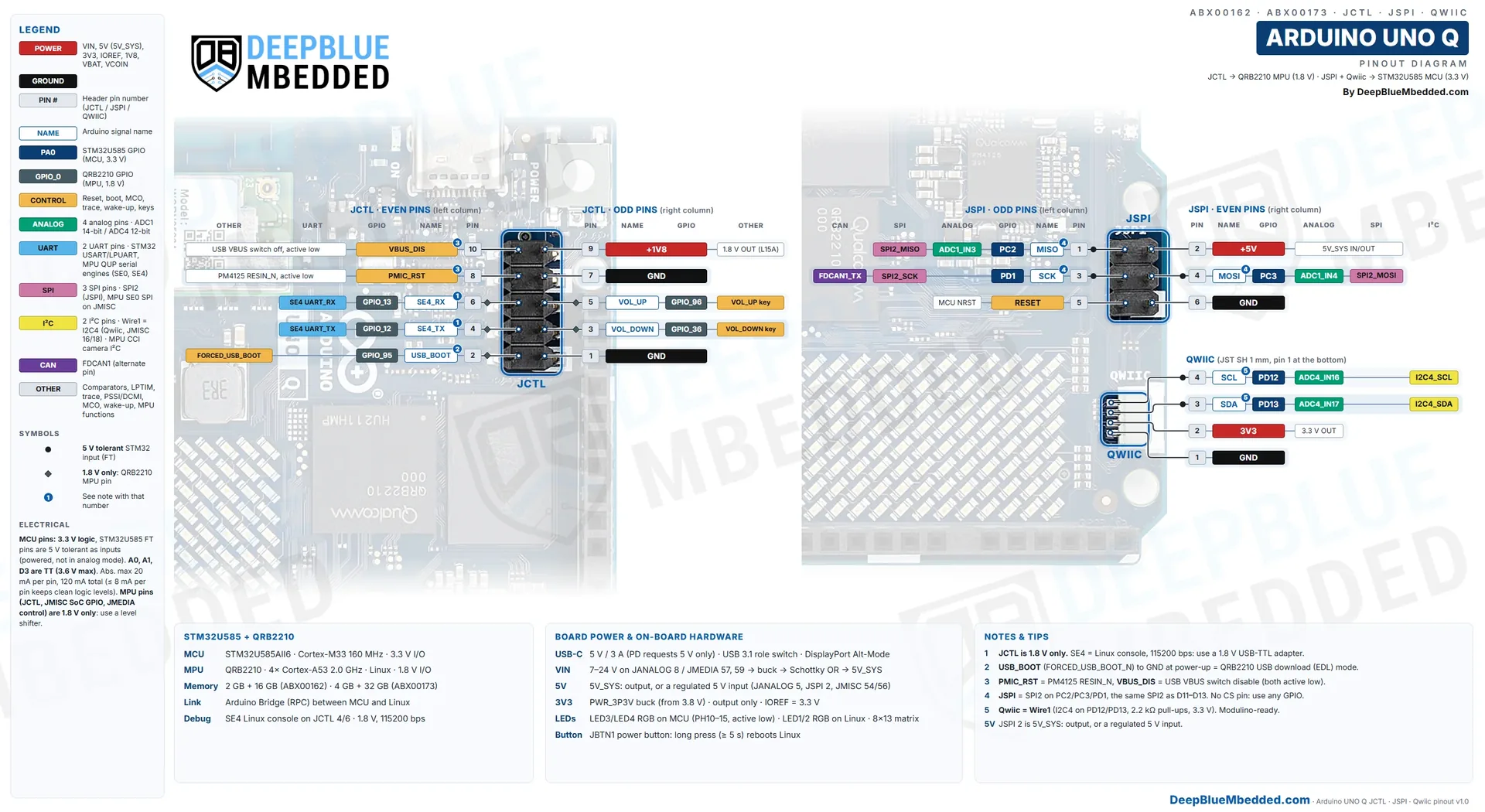
These three small headers sit on the top side. JCTL (2×5, next to the USB-C port) belongs to the Linux processor and runs at 1.8v; JSPI (2×3) and the Qwiic connector belong to the STM32U585 at 3.3v. The PIN column here is the physical connector pin number.
Arduino UNO Q JMISC Pinout (Bottom Side)
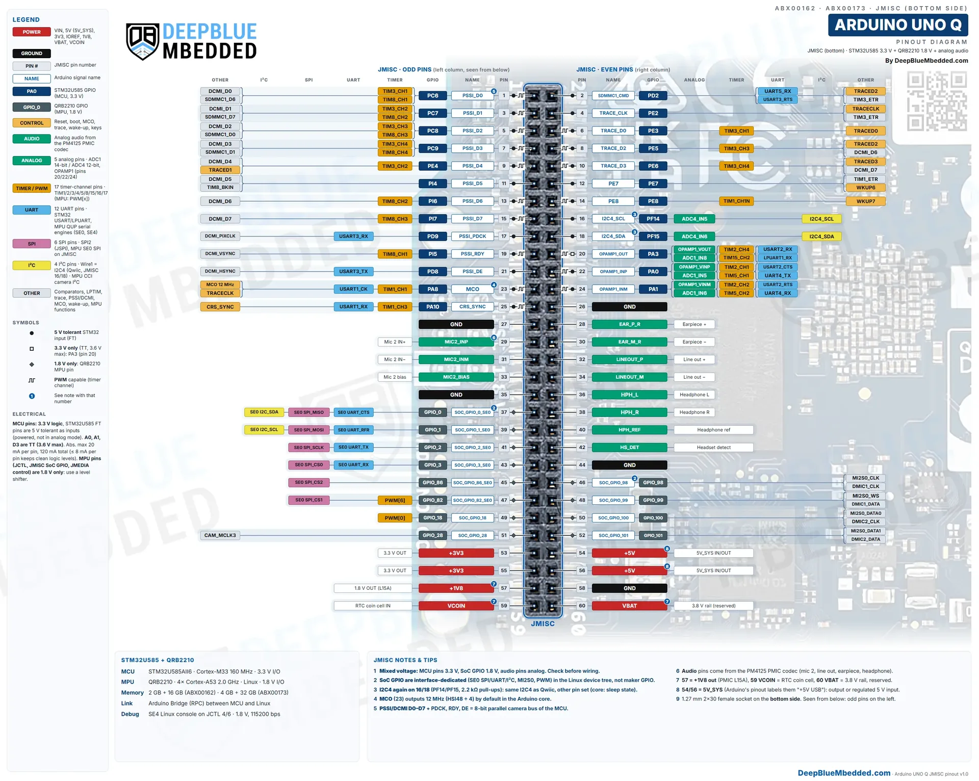
Arduino UNO Q JMEDIA Pinout (Bottom Side)
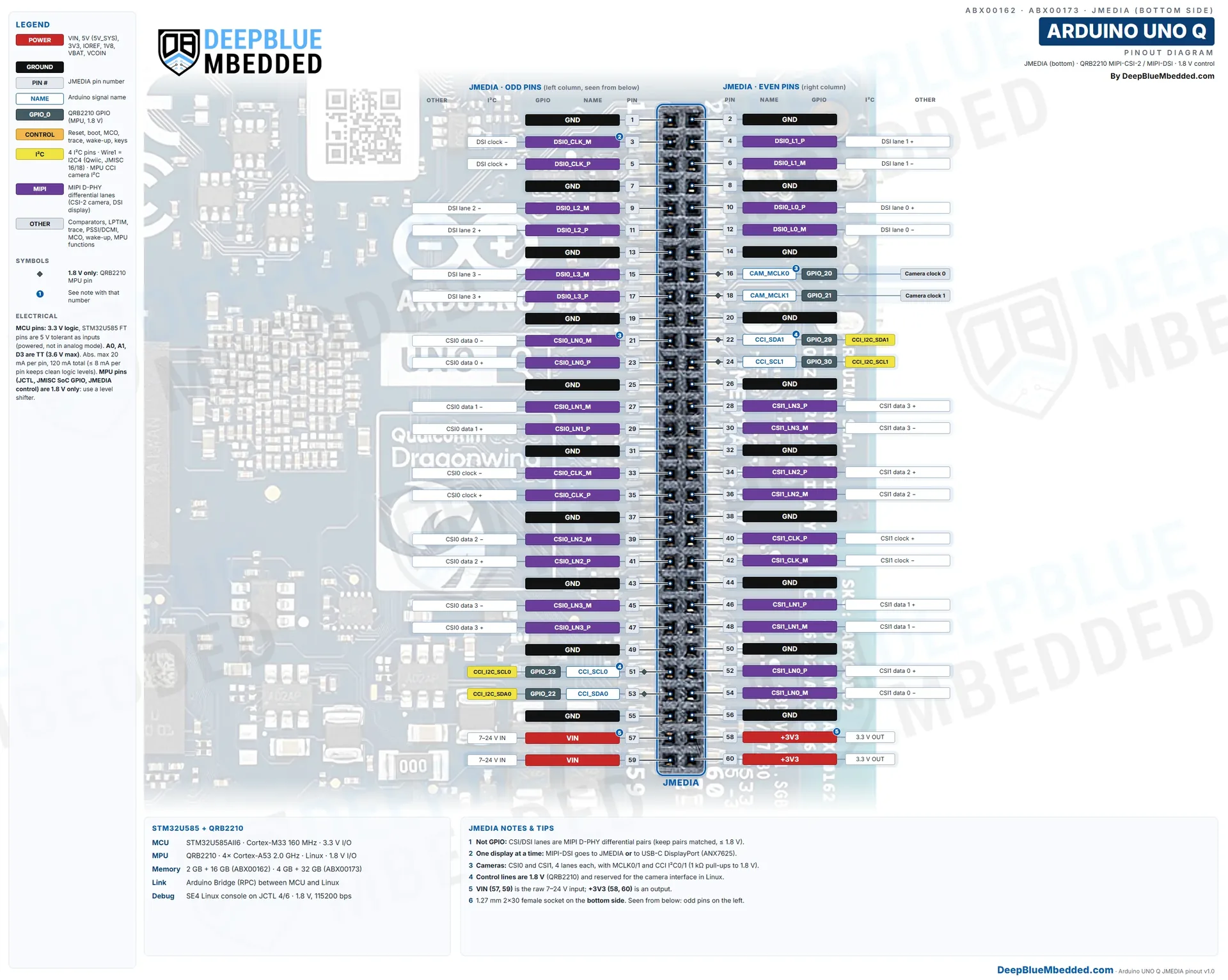
JMISC and JMEDIA are 1.27mm 2×30 female connectors on the bottom side, made for carrier boards. Both diagrams show the board seen from below (as you see it when you flip it over), with pin 1 at the top left, odd pins in the left column and even pins in the right column.
Buy an Arduino UNO Q: If you don’t have one yet, you can get the genuine Arduino board (ABX00162, 2GB/16GB) from Amazon or AliExpress. It runs Linux and Arduino sketches out of the box, so all you need is a 5v/3A USB-C power supply.
Download Arduino UNO Q Pinout Diagrams (Full Resolution)
All 4 Arduino UNO Q pinout diagrams (UNO headers, JCTL/JSPI/Qwiic, JMISC, and JMEDIA) in full resolution, in one ZIP file. Print them, zoom in, or keep them next to your bench. Please consider supporting my work if it helped you.
Arduino UNO Q Datasheet
This development board is built around two chips: the Qualcomm QRB2210 microprocessor and the STM32U585 microcontroller (STM32U585AII6, UFBGA169). So the Arduino UNO Q datasheet set has three parts: Arduino’s documents for the board, ST’s for the microcontroller, and Qualcomm’s for the Linux processor. Here are the official documents you’ll need, linked to their original sources:
| Document | ID | Revision | What You’ll Use It For | Link |
|---|---|---|---|---|
| Arduino UNO Q datasheet (user manual) | ABX00162 / ABX00173 | Rev 16 (30 Oct 2026) | Board specs, power inputs and rails, every connector’s pin map | |
| Arduino UNO Q schematic | ABX00162 | 1 Oct 2025 | The full board circuit (see the next section) | |
| Arduino UNO Q full pinout | ABX00162 | 17 Feb 2026 | Arduino’s 4-page pin map, including JMISC and JMEDIA | |
| Arduino UNO Q user manual (web) | Arduino Docs | Nov 2026 | App Lab, Bridge, ADC, DAC, PWM, Serial, LED matrix examples | Web |
| STM32U585xx datasheet | DS13086 | Rev 10 (Jul 2024) | Pin functions, 5v tolerance (FT/TT), electrical limits | |
| STM32U575/585 errata sheet | ES0499 | Rev 12 (Jun 2026) | Known silicon limitations | ST page |
| QRB2210 data sheet | 80-30843-1 | Rev AE (Oct 2025) | The Linux processor’s GPIO, MIPI, and audio interfaces | Web |
| Dragonwing QRB2210 product brief | 87-61720-1 | Rev D | A two-page summary of the processor |
Which document do I need? The Arduino datasheet for the board’s power inputs and connector pin maps, the schematic for what’s wired to each pin, the STM32U585 datasheet for pin functions and 5v tolerance, and the QRB2210 data sheet only if you work on the 1.8v Linux pins. ST’s reference manual (RM0456, for register-level code) is on the STM32U585 product page, and Arduino keeps every board file on the Arduino UNO Q product page.
Arduino UNO Q Schematic
The Arduino UNO Q schematic is shown below. Most of its sheets are the Qualcomm processor’s internals, so the carousel below shows the 12 sheets that matter when you wire the board: power, the STM32U585, the connectors, and the links between the two processors. Click a page to view it full screen.
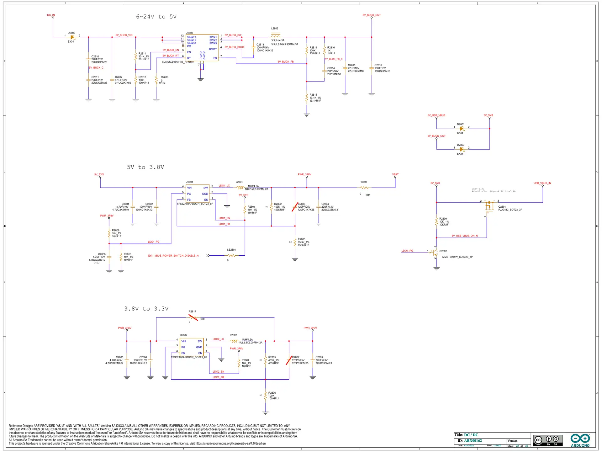
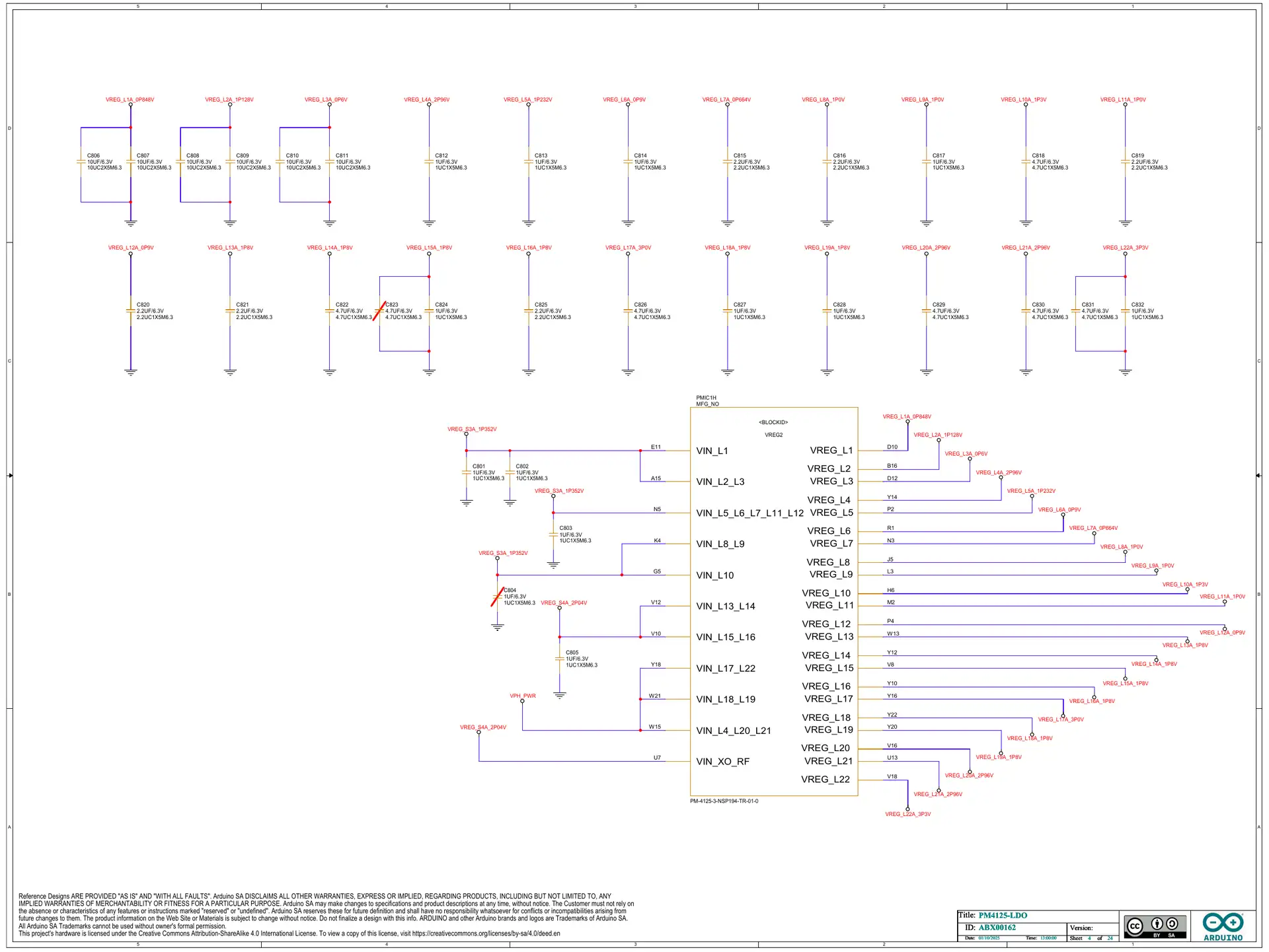
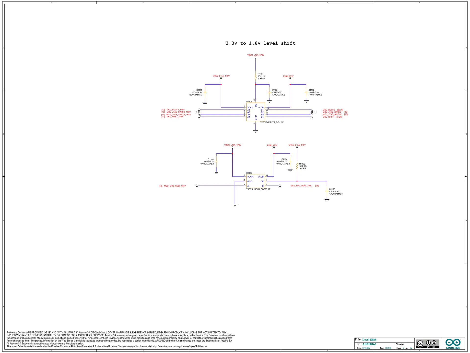
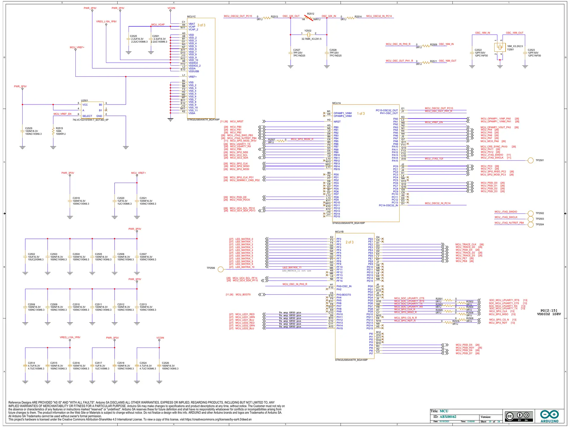
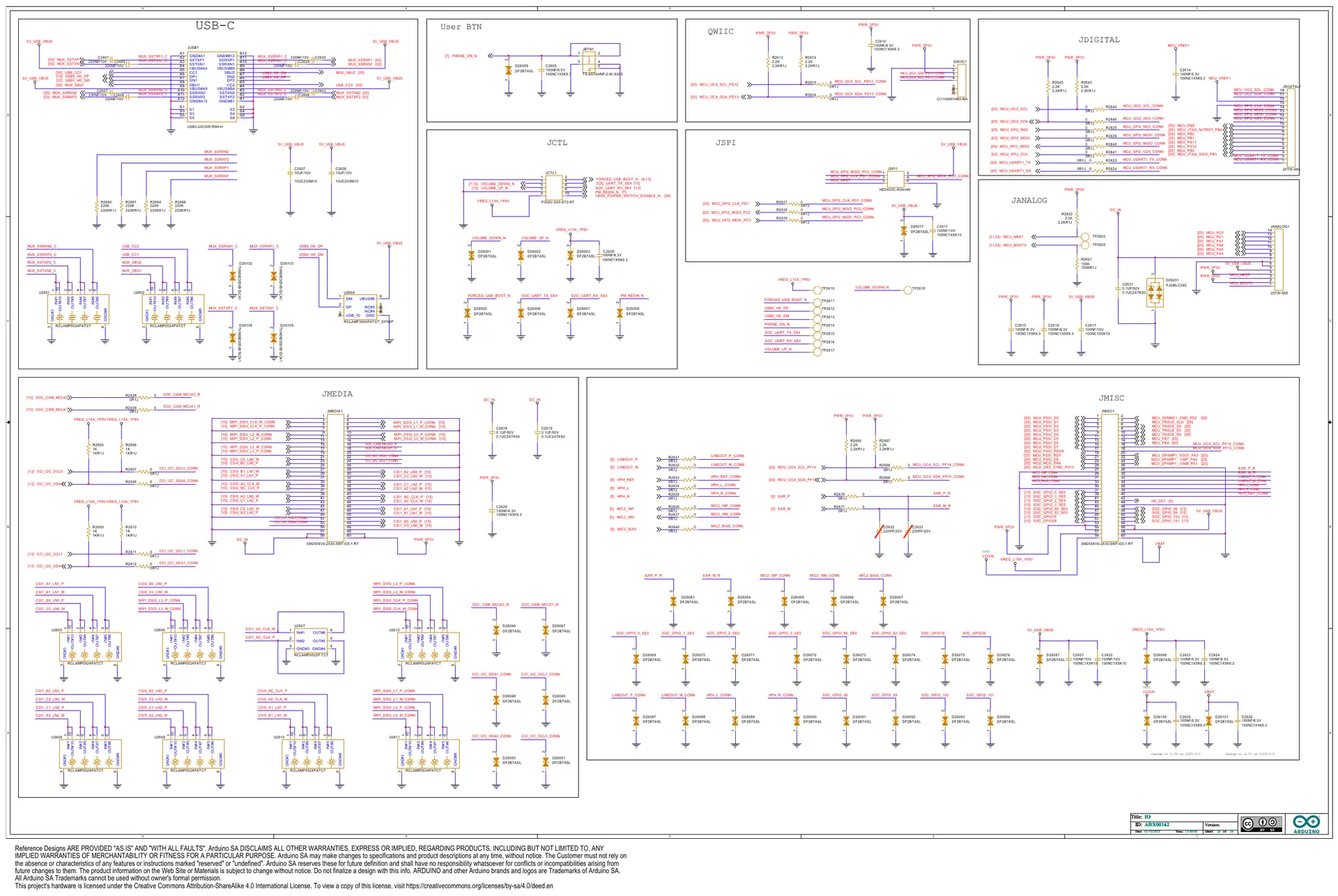
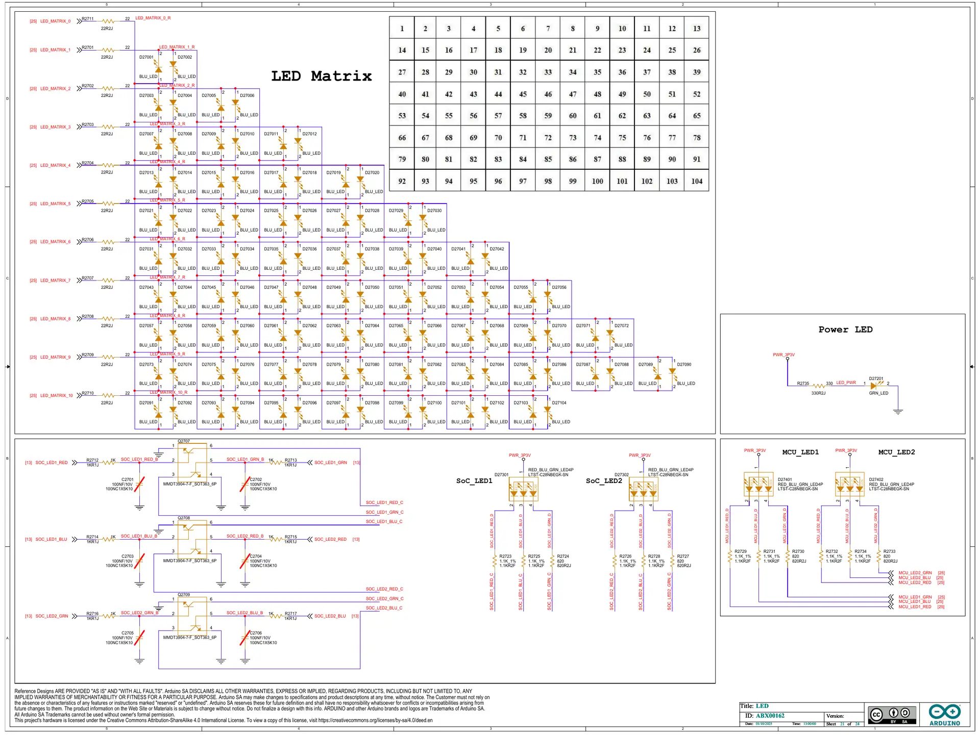
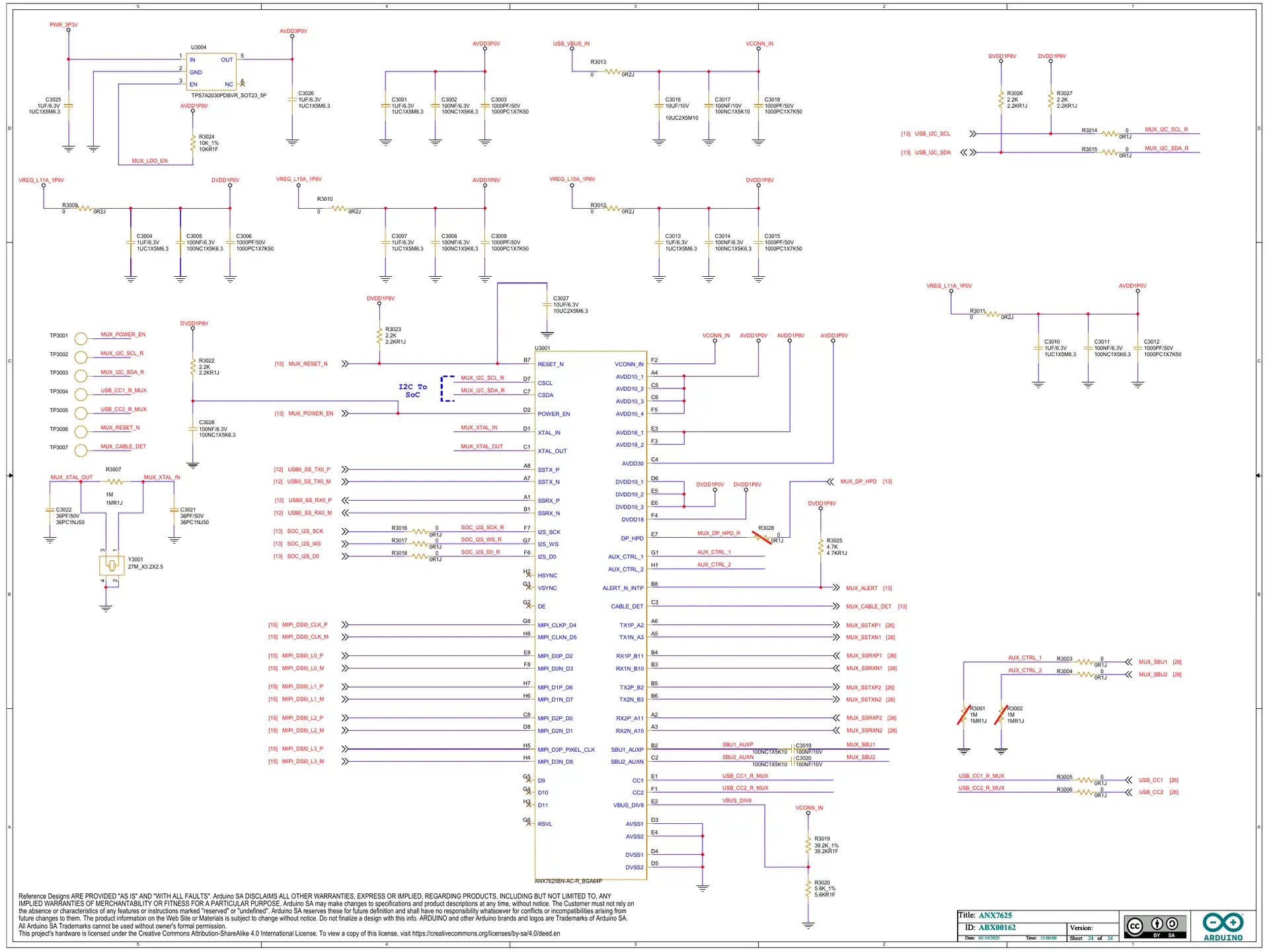
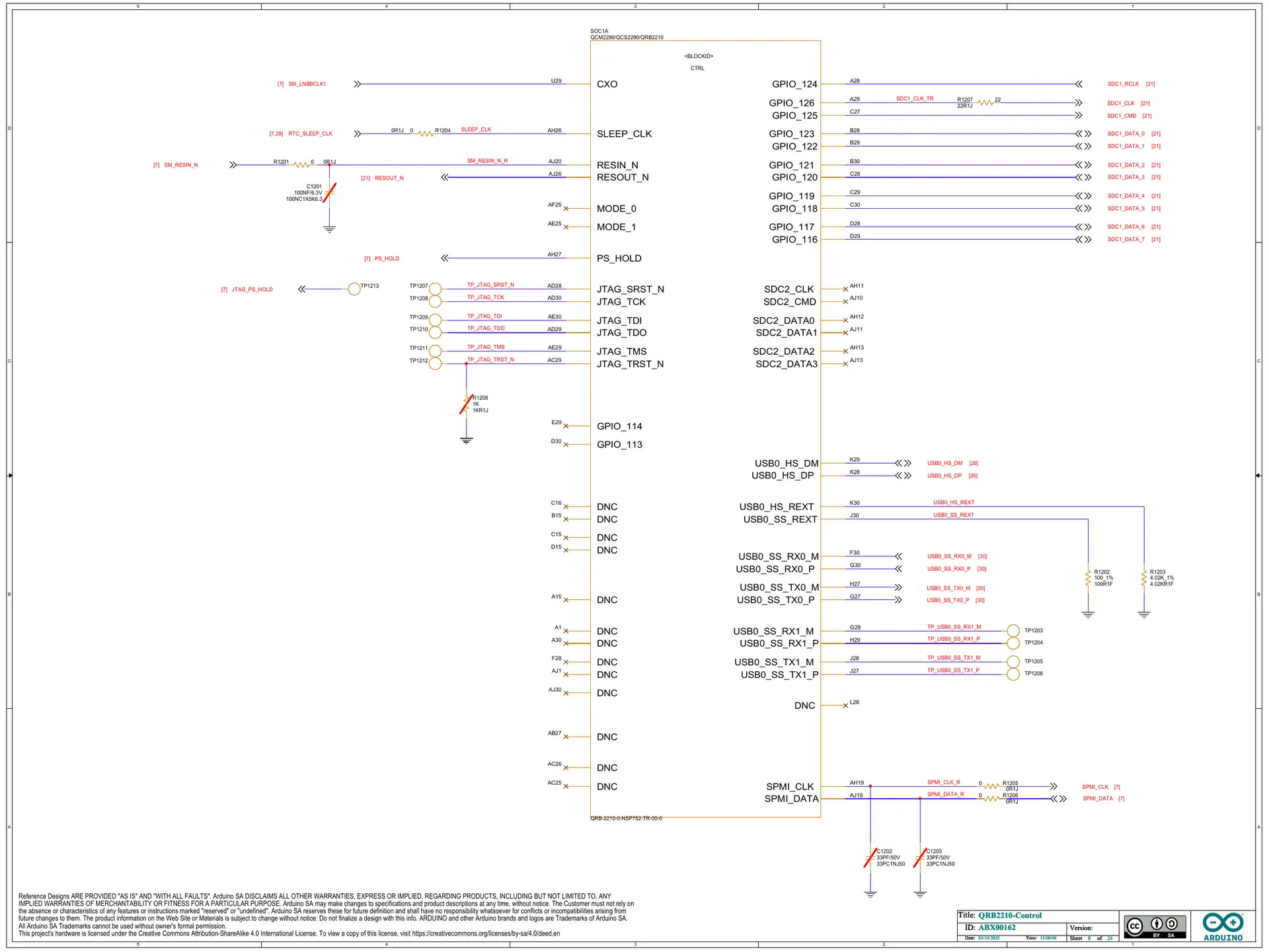
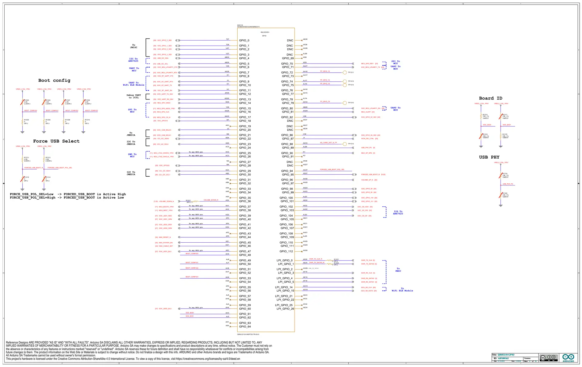
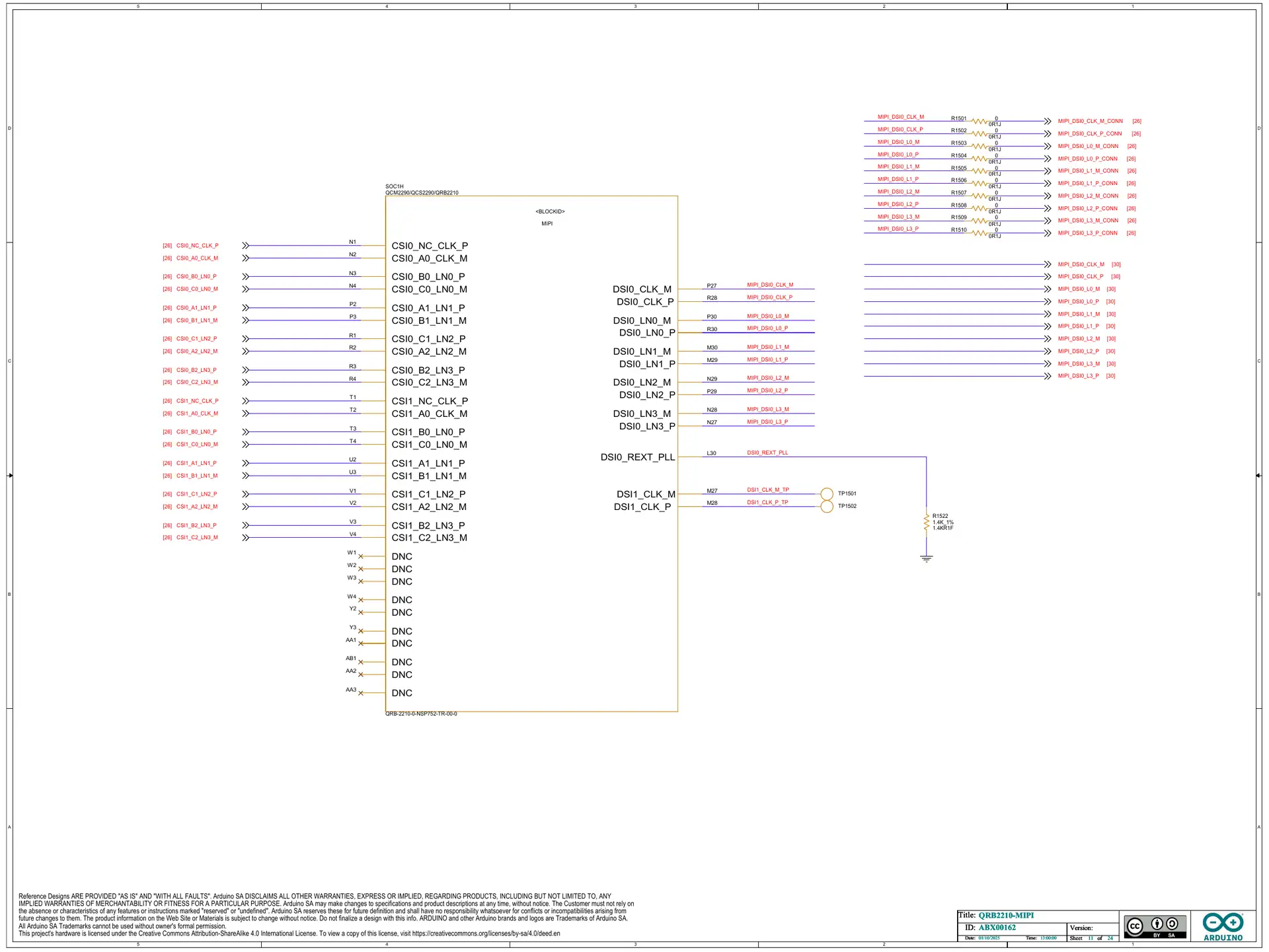
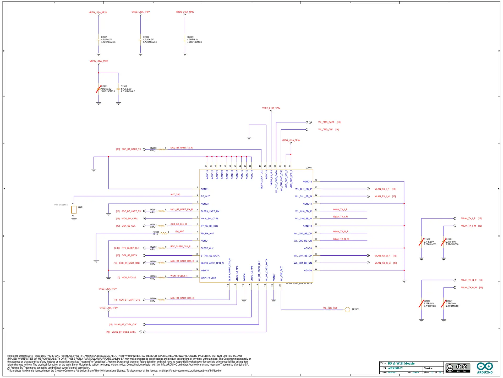
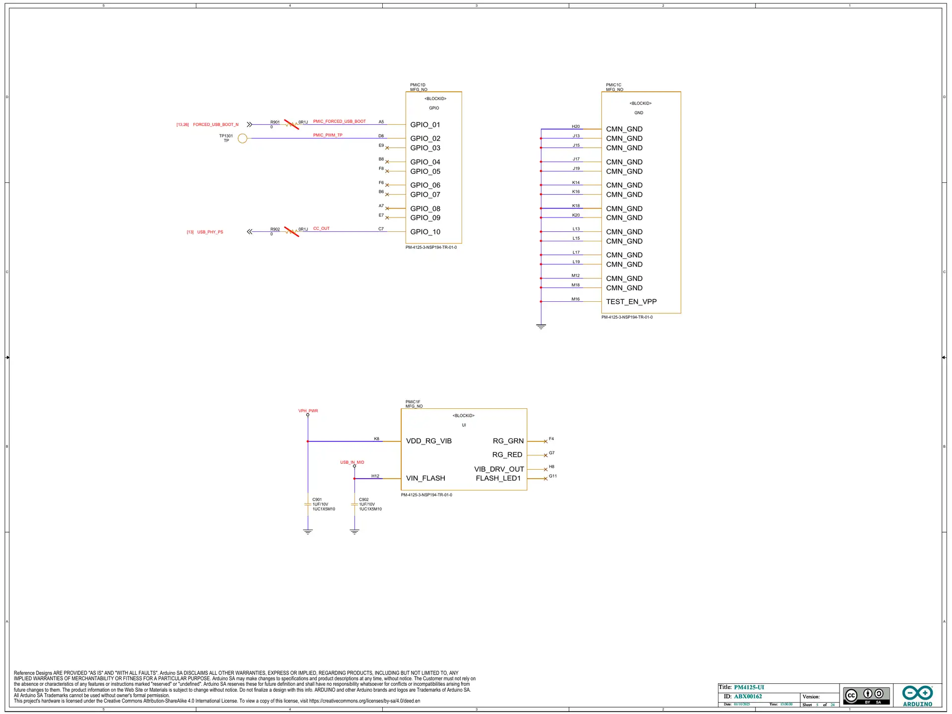
Official source: the Arduino UNO Q schematic (PDF) on Arduino Docs, licensed CC BY-SA 4.0. Here’s what to look at:
- Power path (sheet 22): VIN goes through a reverse-polarity diode into the LMR51440 buck converter, which makes 5v. That 5v and the USB-C VBUS each pass through an SX34 Schottky diode onto 5V_SYS, the board’s main 5v bus (the “diode-OR”). Two TPS62A02 bucks then make 3.8v and 3.3v in a chain, and the Qualcomm PM4125 PMIC makes the 1.8v rail (LDO L15A, sheet 4) from 5V_SYS.
- STM32U585 (sheet 19): it runs from the 3.3v rail, with a 16MHz crystal (Y2501) and a 32.768kHz crystal (Y2502) for the RTC. A 74LVC1G3157 analog switch (U2501), controlled by PA2, selects what feeds the ADC reference VREF+. BOOT0 (PH3) goes to the JANALOG BOOT pin.
- The link between the two processors (sheet 19): the STM32U585’s LPUART1 (with RTS/CTS) and SPI3, both on port G pins, are wired to the QRB2210, and its SWD pins (PA13/PA14) go to the QRB2210 too. That’s how Linux flashes your sketch and how the Bridge library carries data between them.
- Connectors (sheet 20): JANALOG, JDIGITAL, JSPI, JCTL, Qwiic, JMISC and JMEDIA, with the 2.2kΩ pull-ups on the Wire (D20/D21) and Qwiic I2C lines. A4/A5 (Wire2) have no pull-ups.
- LEDs (sheet 21): the 8×13 LED matrix is driven by eleven STM32 pins, PF0–PF10; RGB LED3/LED4 are on PH10–PH15, and RGB LED1/LED2 on QRB2210 GPIOs.
- USB-C and video (sheet 24): the ANX7625 turns the QRB2210’s MIPI-DSI into DisplayPort on the USB-C port. The same DSI lanes go to JMEDIA, and only one of the two can be active at a time.
Note: the full pinout PDF labels JMISC 54/56 as “+5V USB” while the schematic shows 5V_SYS, and the datasheet calls JMISC 57 a 1.8v input while the schematic ties it to the PMIC’s 1.8v output. This article follows the schematic in both cases.
Arduino UNO Q Specs
The Arduino UNO Q is a single-board computer and an Arduino in one. Here are its specifications, including the board-level parts that chip-only spec lists usually skip.
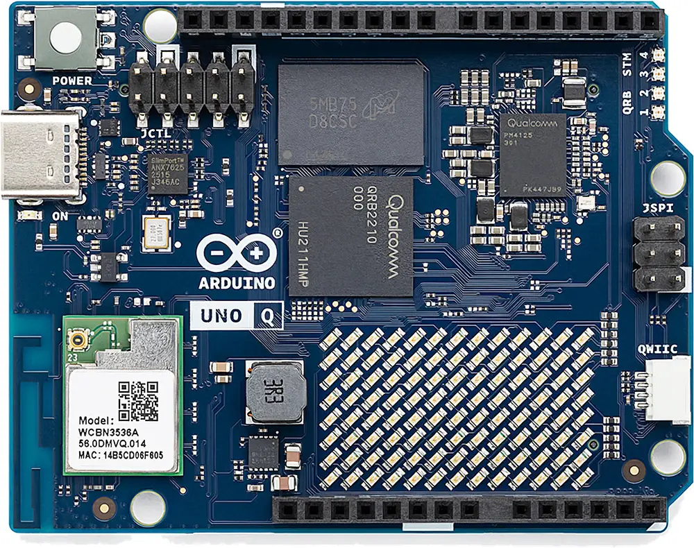
Get an Arduino UNO Q: The genuine Arduino board (ABX00162, 2GB/16GB) is the one I recommend. Grab it from Amazon or AliExpress.
| Item | Arduino UNO Q |
|---|---|
| Microprocessor (MPU) | Qualcomm Dragonwing QRB2210: 4x Arm Cortex-A53 at 2.0GHz, Adreno 702 GPU, Debian Linux |
| Microcontroller (MCU) | ST STM32U585AII6: Arm Cortex-M33 at 160MHz, 2MB flash, 786KB SRAM, Arduino core on Zephyr OS |
| Memory | ABX00162: 2GB LPDDR4X + 16GB eMMC · ABX00173: 4GB LPDDR4X + 32GB eMMC |
| Wireless | WCBN3536A (Qualcomm WCN3980): Wi-Fi 5 dual-band and Bluetooth 5.1 |
| Logic level | 3.3v on the UNO headers, JSPI, and Qwiic (STM32U585); 1.8v on JCTL and the Linux pins of JMISC/JMEDIA |
| MCU I/O on the UNO headers | 22: D0–D13, A0–A5, D20 (SDA), D21 (SCL) |
| Analog | 6 ADC inputs (A0–A5, up to 14-bit), 2x 12-bit DAC (A0, A1) |
| Board supply | USB-C 5v (4.5v–5.5v, up to 3A, PD 5v/3A only), 7v–24v on VIN, or a regulated 5v on the 5V pin |
| Regulators | LMR51440 buck (VIN to 5v), 2x TPS62A02 buck (5v to 3.8v to 3.3v), PM4125 PMIC (1.8v) |
| Pin current (STM32) | 20mA absolute max per pin, 120mA total (DS13086) |
| USB connector | USB-C, USB 3.1 with role switching and DisplayPort Alt-Mode (ANX7625), wired to the QRB2210 |
| Connectors | UNO headers (JANALOG 14-pin, JDIGITAL 18-pin), JCTL 2×5, JSPI 2×3, Qwiic, JMISC 2×30 and JMEDIA 2×30 (bottom, 1.27mm) |
| User I/O | 8×13 blue LED matrix, 4x RGB LEDs (2 for Linux, 2 for the MCU), power LED, power button |
| Clocks (MCU) | 16MHz crystal and 32.768kHz RTC crystal |
| Form factor | Arduino UNO, 68.58 × 53.34mm |
| Operating temperature | −10°C to +60°C (ambient) |
| Order codes | ABX00162 (2GB/16GB), ABX00173 (4GB/32GB); same PCB and pinout |
Arduino UNO Q Specifications Summary
- The Arduino UNO Q has two processors: a QRB2210 (4x Cortex-A53, 2.0GHz, Debian Linux) and an STM32U585 (Cortex-M33, 160MHz, 2MB flash, 786KB SRAM) running your Arduino sketch.
- The STM32U585 owns the UNO headers, JSPI, Qwiic, and the LED matrix; the QRB2210 owns USB-C, Wi-Fi/Bluetooth, JCTL, JMEDIA, and the 1.8v pins of JMISC.
- The UNO header pins run at 3.3v logic, not 5v. Most are 5v tolerant as digital inputs, but A0, A1, and D3 are not (3.6v max).
- It has 6 analog inputs (A0–A5) with a 14-bit ADC and 2 DAC outputs on A0 and A1 (12-bit).
- analogWrite() gives PWM on 13 pins: D2, D3, D5–D13, D20, D21, at a fixed 500Hz.
- Serial goes to Linux (the App Lab console); Serial1 is the hardware UART on D0 (RX) / D1 (TX).
- Wire is on D20 (SDA) / D21 (SCL), Wire1 is the Qwiic connector, and Wire2 is A4 (SDA) / A5 (SCL).
- SPI is D11 (MOSI), D12 (MISO), D13 (SCK) with D10 as SS; JSPI carries the same SPI2 bus.
- The CAN pins are D4 (TX) and D5 (RX) (FDCAN1); they need an external 3.3v CAN transceiver.
- Power it from USB-C 5v/3A or VIN 7v–24v; the 5V pin is the 5V_SYS bus (output, or a regulated 5v input).
- LED_BUILTIN is RGB LED3 (red, PH10), not D13.
- The Linux console is on JCTL pin 4 (TX) and pin 6 (RX) at 1.8v, 115200 bps.
Arduino UNO Q Peripherals: STM32U585 vs On the UNO Headers
The STM32U585 has far more peripherals than the UNO headers can expose, and some of what reaches the headers isn’t used by the Arduino core. This table shows what the chip has, what you can reach, and what the core sets up by default.
| Peripheral | STM32U585 | On the UNO Headers | Arduino Core Default |
|---|---|---|---|
| ADC | ADC1 14-bit + ADC4 12-bit | ADC1 on A0–A5, D3, D6, D7 | analogRead() on A0–A5 |
| DAC | 2x 12-bit | A0 (DAC1_OUT1), A1 (DAC1_OUT2) | analogWrite(DAC0/DAC1, …) |
| Op-amp | 2 | OPAMP2 on A2 (+), A3 (−), D3 (out); OPAMP1 on JMISC | Not used by the core |
| PWM timers | TIM1/8 advanced, TIM2/3/4/5, TIM15/16/17, LPTIM1–4 | 18 pins with a timer channel | 13 pins at 500Hz |
| UART | 3x USART, 2x UART, 1x LPUART | USART1 (D0/D1), USART3 (D20/D21), LPUART1 (A4/A5 alt.) | Serial1 = USART1, Serial3 = USART3 |
| SPI | 3 | SPI2 (D10–D13 and JSPI), SPI1 (alt.) | SPI = SPI2 |
| I2C | 4 | I2C2 (D20/D21), I2C3 (A4/A5), I2C1/I2C4 (alt.) | Wire = I2C2, Wire1 = I2C4 (Qwiic), Wire2 = I2C3 |
| CAN | 1x FDCAN | D4 (TX), D5 (RX) | FDCAN1 on D4/D5 |
| USB | USB OTG FS (PA11/PA12) | Not available: PA11/PA12 are D5/D4 | The board’s USB-C belongs to the QRB2210 |
Arduino UNO Q Quick Pin Selection Guide
Not sure which pin to use? Here are the Arduino UNO Q pins I’d pick first for each job, and why.
| Use Case | Recommended Pins | Why |
|---|---|---|
| Print debug messages | Serial (Monitor) | Shows up in the App Lab console over the Bridge |
| Serial to a module (GPS, GSM…) | D0 (RX), D1 (TX) as Serial1 | The UNO-position hardware UART (mind the boot banner) |
| I2C sensors and displays | D20 (SDA), D21 (SCL) as Wire | The default bus, with 2.2kΩ pull-ups on board |
| Qwiic / STEMMA QT / Modulino | Qwiic connector as Wire1 | Plug-and-play, 3.3v, pull-ups on board |
| Old shields with I2C on A4/A5 | A4 (SDA), A5 (SCL) as Wire2 | Add your own pull-ups |
| SPI devices | D11 (MOSI), D12 (MISO), D13 (SCK), D10 (SS) | The default SPI pins |
| Analog inputs | A2–A5 | A0/A1 are not 5v tolerant and double as DAC outputs |
| True analog output | A0 (DAC0), A1 (DAC1) | 12-bit DACs, a real voltage instead of PWM |
| PWM (LEDs, motors) | D3, D5, D6, D9, D10, D11 | The “~” pins, each on its own timer channel |
| CAN bus | D4 (TX), D5 (RX) | FDCAN1; add a 3.3v transceiver |
| Safest general GPIO | D2, D6, D7, D8, D9 | No bus, boot, or analog role by default |
| Linux console | JCTL 4 (TX), JCTL 6 (RX) | 1.8v UART; use a 1.8v USB-TTL adapter |
Arduino UNO Q Pins to Use With Caution
| Pin | Reason | What to Do |
|---|---|---|
| A0, A1, D3 | Not 5v tolerant (TT pins, 3.6v max) | Never connect a 5v signal; use a divider or level shifter |
| All UNO header pins | 3.3v logic: outputs only reach 3.3v | Level-shift 5v modules that need a 5v HIGH |
| A0–A5 in analog mode | Analog inputs are limited to VDD + 0.3v | Keep analog signals within 0v–3.3v |
| BOOT (JANALOG 1) | STM32 BOOT0: HIGH at reset starts the ST bootloader | Leave it open (it has a 100kΩ pull-down) |
| D0, D1 | Serial1, and Zephyr prints its boot log there | Ignore the boot text, or use another pin for sensitive inputs |
| D20, D21 | Wire, Serial3, and PWM on the same pins | Pick one role |
| D10–D13 and JSPI | Both are SPI2 | Use one or the other |
| JCTL, JMISC 37–52, JMEDIA | QRB2210 pins at 1.8v | Never connect 3.3v or 5v logic directly |
| JCTL 2 (USB_BOOT) | LOW at power-up forces the QRB2210 into USB download mode | Leave it open in normal use |
| JMISC 20 (PA3) | Not 5v tolerant (TT) | Keep it at 3.3v or below |
Arduino UNO Q MPU vs MCU: Which Processor Owns Which Pins
The Arduino UNO Q’s STM32U585 (MCU) owns the UNO headers, JSPI, the Qwiic connector, the LED matrix, RGB LED3/LED4, and the MCU pins of JMISC (1–25). The QRB2210 (MPU) owns the USB-C port, Wi-Fi and Bluetooth, JCTL, all of JMEDIA, the 1.8v GPIO and audio pins of JMISC, and RGB LED1/LED2. Your Arduino sketch runs on the MCU; Python and Linux apps run on the MPU.
| Connector / Part | Driven By | Logic Level | What’s on It |
|---|---|---|---|
| JANALOG, JDIGITAL (UNO headers) | STM32U585 | 3.3v | D0–D13, A0–A5, D20/D21, power pins |
| JSPI | STM32U585 | 3.3v | SPI2 (MISO, MOSI, SCK), 5V, RESET, GND |
| Qwiic | STM32U585 | 3.3v | I2C4 (Wire1) |
| JMISC 1–25 | STM32U585 | 3.3v | PSSI/camera parallel bus, trace, OPAMP1, I2C4, MCO |
| JMISC 28–52 | QRB2210 + audio codec | 1.8v / analog | Headphone, earpiece, line out, mic, SE0 GPIO, I2S, PWM |
| JMEDIA | QRB2210 | MIPI / 1.8v | 2x MIPI-CSI camera, 1x MIPI-DSI display, camera I2C and clocks |
| JCTL | QRB2210 + PMIC | 1.8v | Linux console UART, USB boot, volume keys, PMIC reset |
| USB-C | QRB2210 | – | USB 3.1, power input, DisplayPort output |
| LED matrix, LED3, LED4 | STM32U585 | – | Sketch-controlled LEDs |
| LED1, LED2 | QRB2210 | – | Linux status LEDs (user, panic, Wi-Fi, Bluetooth) |
The two processors talk through Arduino’s Bridge, an RPC (Remote Procedure Call) library that runs on both sides. On the board, Bridge travels over the MCU’s LPUART1 and SPI3, which are wired straight to the QRB2210 and never reach a header. A sketch can call a Python function on Linux (or the other way round), and the Serial object you print to is also carried by Bridge to the App Lab console. Linux also flashes your sketch into the STM32U585 over SWD, so there’s no programmer and no bootloader to manage.
Note: Never wire a 1.8v QRB2210 pin straight to a 3.3v STM32 pin or module. If you want a hardware signal between the two sides on a carrier board (a “ready” or wake line, for example), Arduino’s datasheet says to use a level shifter, or an open-drain output with a pull-up to the receiving side’s rail.
Arduino UNO Q Pins Functions
The 32 UNO header pins of the Arduino UNO Q are divided into the following groups based on the hardware functionality they’re used for. Most I/O pins belong to several groups at once.
- Power Pins: VIN, 5V, 3V3, IOREF, 3x GND, plus the power pins on JSPI, JMISC, and JMEDIA
- 22x Digital GPIO Pins (D0–D13, A0–A5, D20, D21)
- Interrupt Pins
- 6x ADC Analog Input Pins
- 2x DAC Pins
- 13x PWM Pins
- 2x UART Ports (+ Serial over Bridge)
- 3x I2C Buses (D20/D21, Qwiic, A4/A5)
- 1x SPI Port (D10–D13 or JSPI)
- 1x CAN Bus
- USB-C Port
- BOOT, Reset & Debug Pins (JANALOG and JCTL)
- JMISC & JMEDIA Pins (camera, display, audio)
We’ll discuss each pin group in the following sections one by one in more detail.
Arduino UNO Q Power Pins
The Arduino UNO Q is powered from USB-C (5v, up to 3A), from 7v–24v on VIN, or from a regulated 5v on the 5V pin. USB-C and the VIN buck converter meet on 5V_SYS through Schottky diodes, and every other rail (3.8v, 3.3v, 1.8v) is made from 5V_SYS. The power pins are highlighted in red in the pinout diagram.
| Pin | Where | Range | Notes |
|---|---|---|---|
| VIN | JANALOG 8, JMEDIA 57/59 | 7v–24v in | LMR51440 buck to 5v, then Schottky diode to 5V_SYS; reverse polarity tested to −24v |
| 5V | JANALOG 5, JSPI 2, JMISC 54/56 | 5v | 5V_SYS: an output, or a regulated 5v input |
| 3V3 | JANALOG 4, Qwiic 2, JMISC 53/55, JMEDIA 58/60 | 3.3v out (3.1v–3.5v) | TPS62A02 buck from the 3.8v rail; output only |
| IOREF | JANALOG 2 | 3.3v out | Tells shields the board runs at 3.3v |
| +1V8 | JCTL 9, JMISC 57 | 1.8v out | PM4125 LDO L15A; a reference for 1.8v level shifters |
| GND | JANALOG 6, 7, JDIGITAL 15, and every connector | 0v | All grounds are common |
| VCOIN | JMISC 59 | Coin cell in | Keeps the PMIC’s RTC running |
| VBAT | JMISC 60 | 3.8v rail | The board’s 3.8v pre-regulator node; Arduino lists it as reserved |
Over USB Power Delivery the board asks only for 5v/3A, never a higher voltage, so use a supply and cable rated for 3A: short current peaks (Wi-Fi bursts, a display starting up) can reset the board on a weak supply. On VIN, the Schottky diode drops about 0.35v–0.39v at 1A–2A, which Arduino measured and lists in the datasheet.
Note: Arduino doesn’t publish a current limit for the 3V3 and 5V pins as outputs. So, to stay on the safe side, keep big loads (motors, LED strips, servos) on their own supply, and share only GND with the Arduino UNO Q.
Arduino UNO Q GPIO Pins
The Arduino UNO Q has 22 GPIO pins on its UNO headers: D0–D13, A0–A5 (digital pins 14–19), and D20/D21 (the SDA/SCL pins). They’re STM32U585 pins at 3.3v logic, so an output HIGH is 3.3v, not 5v. That’s the biggest change from the UNO R3.
Each pin can be INPUT, INPUT_PULLUP, or OUTPUT. Here are the limits that matter, from ST’s DS13086 and Arduino’s datasheet:
- 5v tolerance: most UNO pins are STM32 “FT” pins, which accept 5v as a digital input while the board is powered. A0 (PA4), A1 (PA5), and D3 (PB0) are “TT” pins: 3.6v max, never 5v. Arduino’s pinout PDF only warns about A0/A1; D3 is in the datasheet and in Arduino’s GitHub issue #2908.
- In analog mode, no pin is 5v tolerant: analog inputs must stay below VDD + 0.3v (about 3.6v).
- Current: 20mA absolute maximum per pin and 120mA for all pins together (DS13086 Table 21). Plan on a few mA per pin for clean logic levels.
- The JSPI and JMISC MCU pins also have Arduino numbers: JSPI MISO, MOSI, SCK are 22, 23, 24, and the JMISC MCU pins are 25–49 (the JMISC pin number + 24).
Note: 5v tolerant doesn’t mean 5v compatible. A 5v module reading the Arduino UNO Q’s 3.3v output may not see it as HIGH, and a 5v I2C or UART device can still pull a pin above its limit through its own pull-ups. Use a level shifter for 5v modules, as users found with UNO shields on the Arduino Forum.
Learn more in our Arduino digitalWrite() GPIO Tutorial.
Also Read
Arduino UNO Q Interrupt Pins
Arduino hasn’t published a list of interrupt pins for the Arduino UNO Q. attachInterrupt() uses the STM32U585’s EXTI lines, and the STM32 has one EXTI line per pin number (line 0 for PA0, PB0, PC0…), so any GPIO can trigger an interrupt, but two pins with the same number can’t both be interrupts at once. I haven’t tested every pin on hardware, so treat the table below as the STM32 rule applied to the UNO headers.
| EXTI Line | UNO Pins Sharing It | Pick One |
|---|---|---|
| 0 | D3 (PB0), A5 (PC0) | D3 or A5 |
| 1 | D6 (PB1), A4 (PC1) | D6 or A4 |
| 4 | D8 (PB4), A0 (PA4) | D8 or A0 |
| 6 | D1 (PB6), A2 (PA6) | D1 or A2 |
| 7 | D0 (PB7), A3 (PA7) | D0 or A3 |
| 11 | D5 (PA11), D20 (PB11) | D5 or D20 |
Every other UNO pin (D2, D4, D7, D9–D13, A1, D21) has its EXTI line to itself on the headers. So D2 and D4 make a good pair for two buttons or an encoder.
|
1 2 3 4 5 6 7 8 9 10 11 12 |
volatile bool pressed = false; void onPress() { pressed = true; } void setup() { pinMode(LED_BUILTIN, OUTPUT); pinMode(2, INPUT_PULLUP); // button from D2 to GND attachInterrupt(digitalPinToInterrupt(2), onPress, FALLING); } void loop() { if (pressed) { pressed = false; digitalWrite(LED_BUILTIN, !digitalRead(LED_BUILTIN)); } } |
Learn more in our Arduino External Interrupts Tutorial.
Also Read
Arduino UNO Q ADC Pins
The Arduino UNO Q has 6 ADC pins, A0–A5, on the STM32U585’s 14-bit ADC1. analogRead() returns 10-bit values (0–1023) by default, and analogReadResolution() accepts 8, 10, 12, or 14 bits. The input range is 0v to 3.3v. The ADC pins are highlighted in green in the pinout diagram.
| Pin | STM32 Pin | ADC Channel | Also | 5v Tolerant |
|---|---|---|---|---|
| A0 | PA4 | ADC1_IN9 | DAC0 output | No (3.6v max) |
| A1 | PA5 | ADC1_IN10 | DAC1 output | No (3.6v max) |
| A2 | PA6 | ADC1_IN11 | OPAMP2 + input | Digital mode only |
| A3 | PA7 | ADC1_IN12 | OPAMP2 − input | Digital mode only |
| A4 | PC1 | ADC1_IN2 | Wire2 SDA | Digital mode only |
| A5 | PC0 | ADC1_IN1 | Wire2 SCL | Digital mode only |
The default reference is the 3.3v rail. analogReference() also accepts the STM32’s internal reference buffer, AR_INTERNAL1V5, AR_INTERNAL1V8, AR_INTERNAL2V05, or AR_INTERNAL2V5 ( AR_INTERNAL = 2.5v), and AR_EXTERNAL for a reference on the AREF pin (from the core’s variant file). Let’s say you read a 0v–1v sensor: with the 3.3v reference and 14-bit resolution, it uses about 4,965 steps; with the 1.5v reference, it uses about 10,923.
Note: D3, D6, and D7 also have ADC1 channels in the STM32 (the diagram shows them), but the Arduino core only maps analogRead() to A0–A5. Stay with A0–A5 for analog inputs.
There are so many sensors that we can read with the ADC pins, which include: potentiometers, LDRs, analog temperature sensors (TMP36, NTC thermistors), soil moisture sensors, joysticks, current sensors, and much more.
|
1 2 3 4 5 6 7 8 9 10 11 |
void setup() { Serial.begin(115200); // goes to the App Lab console analogReadResolution(14); // 0..16383 } void loop() { int raw = analogRead(A2); float volts = raw * 3.3 / 16383.0; // default 3.3v reference Serial.println(volts, 3); delay(500); } |
Learn more in our Arduino ADC analogRead() Tutorial.
Also Read
Arduino UNO Q DAC Pins
The Arduino UNO Q has 2 DAC outputs: DAC0 on A0 (PA4) and DAC1 on A1 (PA5), both 12-bit. analogWrite(DAC0, value) gives a real analog voltage from 0v to 3.3v, not a PWM square wave. The classic UNO R3 has no DAC at all.
| DAC | Pin | STM32 Signal | Range |
|---|---|---|---|
| DAC0 | A0 | PA4 (DAC1_OUT1) | 0v–3.3v, up to 12-bit |
| DAC1 | A1 | PA5 (DAC1_OUT2) | 0v–3.3v, up to 12-bit |
|
1 2 3 4 5 6 7 8 9 10 |
void setup() { analogWriteResolution(12); // 0..4095 } void loop() { for (int i = 0; i < 4096; i += 16) { analogWrite(DAC0, i); // ramp on A0 delayMicroseconds(100); } } |
The STM32U585 also has two op-amps. OPAMP2 sits on A2 (+), A3 (−), and D3 (output), and OPAMP1 on JMISC 22, 24, and 20, but the Arduino core doesn’t set them up, so you’d need register-level code to use them.
Arduino UNO Q PWM Pins
The Arduino UNO Q can output PWM on 13 pins with analogWrite(): D2, D3, D5, D6, D7, D8, D9, D10, D11, D12, D13, D20, and D21, all at a fixed 500Hz (from the core’s variant file). The PWM pins are highlighted in orange in the pinout diagram.
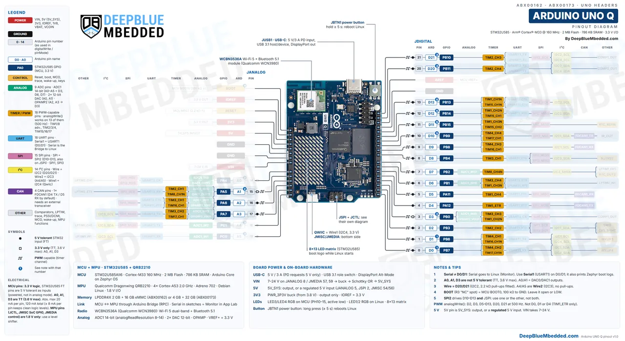
Arduino UNO Q Default PWM Pins: D3, D5, D6, D9, D10, and D11 (the “~” pins), plus D2, D7, D8, D12, D13, D20, and D21.
| Pin | Timer Channel | Pin | Timer Channel |
|---|---|---|---|
| D2 | TIM2_CH2 | D9 | TIM4_CH3 |
| D3 | TIM3_CH3 | D10 | TIM4_CH4 |
| D5 | TIM1_CH4 | D11 | TIM1_CH3N |
| D6 | TIM3_CH4 | D12 | TIM1_CH2N |
| D7 | TIM8_CH4N | D13 | TIM1_CH1N |
| D8 | TIM3_CH1 | D20 / D21 | TIM2_CH4 / TIM2_CH3 |
D0, D1, and D4 have no PWM in the core: D0/D1 are the Serial1 UART, and D4 only has a timer trigger input. D20/D21 are also the Wire I2C pins, so use them for PWM only when you don’t need I2C. The frequency is fixed at 500Hz in the core, so use the Servo library for servos rather than analogWrite().
Note: analogWrite(LED_BUILTIN, …) works too: RGB LED3 (red, green, blue on PH10–PH12) is driven by TIM5, so you can dim or mix colors. LED3 is active LOW, and the core already inverts it for you.
There are so many things that we can control with PWM, which include: LED dimming, RGB LEDs, DC motor speed (with a driver), buzzers, fans, and much more.
Learn more in our Arduino PWM analogWrite() Tutorial.
Also Read
Arduino UNO Q UART Pins
The Arduino UNO Q has 2 hardware UARTs on its UNO headers: Serial1 on D0 (RX) / D1 (TX) (USART1) and Serial3 on D20 (RX) / D21 (TX) (USART3). Serial is not a pin at all: it’s carried by the Bridge to the Linux side and shows up in the App Lab console. The UART pins are highlighted in blue in the pinout diagram.
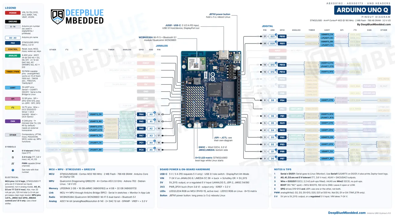
Arduino UNO Q Default UART Pins: D0 (RX) and D1 (TX) for Serial1.
| Arduino Object | Peripheral | RX Pin | TX Pin | Note |
|---|---|---|---|---|
Serial | LPUART1 + Bridge | – | – | To Linux and the App Lab console |
Serial1 | USART1 | D0 (PB7) | D1 (PB6) | Also the Zephyr console (boot messages) |
Serial2 | LPUART1 | – | – | Internal link to the QRB2210; don’t use it |
Serial3 | USART3 | D20 (PB11) | D21 (PB10) | Shares pins with Wire |
| Linux console | QRB2210 SE4 | JCTL 6 | JCTL 4 | 1.8v, 115200 bps |
Serial1 works as a normal UART, with one surprise: the Zephyr OS under the Arduino core prints its boot messages on USART1, so after every MCU reset a few lines of text come out of D1 before your sketch starts (Arduino Forum). A module on D0/D1 should ignore them, or start listening a moment after boot.
|
1 2 3 4 5 6 7 8 |
void setup() { Serial.begin(115200); // App Lab console (through the Bridge) Serial1.begin(9600); // D0 = RX, D1 = TX } void loop() { while (Serial1.available()) Serial.write(Serial1.read()); // module -> console } |
Note: Sketches written for the UNO R3 use Serial on D0/D1. On the UNO Q, change them to Serial1, or the module gets nothing. And the UNO Q’s TX is 3.3v: most 5v modules read it fine, but a 5v module’s TX into D0 is only safe because D0 is a 5v-tolerant pin.
There are so many modules that we can interface with the UART pins, which include: GPS modules, GSM/LTE modules, fingerprint sensors, RS485 transceivers, DFPlayer Mini, other microcontrollers, and much more.
Learn more in our Arduino UART Serial Communication Tutorial.
Arduino UNO Q I2C Pins
The Arduino UNO Q has 3 I2C buses in the Arduino core. Wire is on D20 (SDA) / D21 (SCL) (I2C2), Wire1 is the Qwiic connector (I2C4), and Wire2 is on A4 (SDA) / A5 (SCL) (I2C3). Unlike the UNO R3 and R4, A4/A5 are not connected to the SDA/SCL pins: they’re separate STM32 pins and a separate bus. The I2C pins are highlighted in yellow in the pinout diagram.
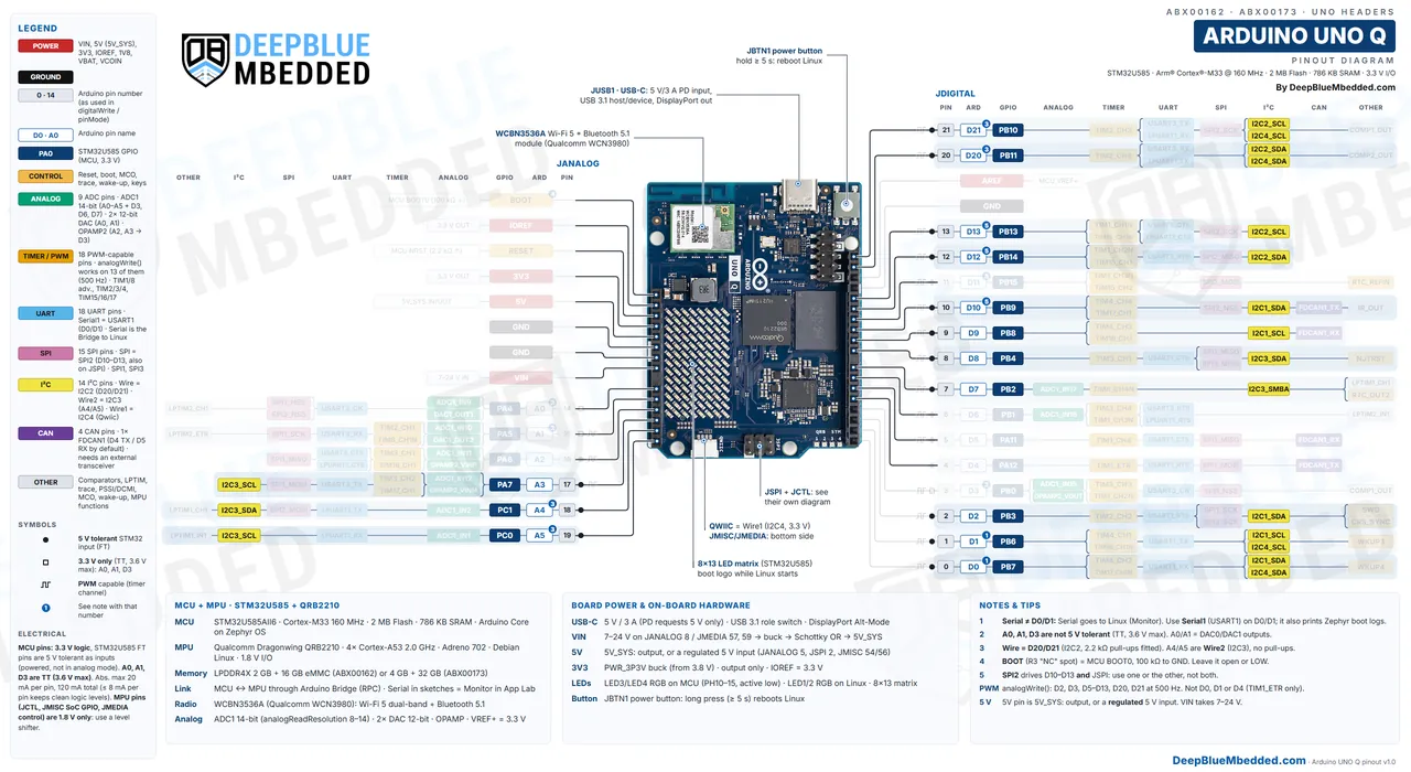
Arduino UNO Q Default I2C Pins: D20 (SDA) and D21 (SCL) for Wire; the Qwiic connector for Wire1.
| Arduino Object | Peripheral | SDA | SCL | Pull-ups on Board |
|---|---|---|---|---|
Wire | I2C2 | D20 (PB11) | D21 (PB10) | 2.2kΩ to 3.3v |
Wire1 | I2C4 | Qwiic 3 (PD13) | Qwiic 4 (PD12) | 2.2kΩ to 3.3v |
Wire2 | I2C3 | A4 (PC1) | A5 (PC0) | None |
The Qwiic connector is a JST SH 4-pin in the standard order: GND, 3.3v, SDA, SCL, so it works with SparkFun Qwiic, Adafruit STEMMA QT, and Arduino Modulino boards. JMISC 16 and 18 are also labelled I2C4 (PF14/PF15) in Arduino’s pinout, but the core only switches them in as an alternate pin set that isn’t enabled yet (a “TODO” in the variant file), so I’d treat them as unconfirmed for now.
|
1 2 3 4 5 6 7 8 9 10 11 12 |
#include <Wire.h> void setup() { Serial.begin(115200); Wire1.begin(); // Qwiic connector for (byte a = 1; a < 127; a++) { Wire1.beginTransmission(a); if (Wire1.endTransmission() == 0) { Serial.print("Qwiic device at 0x"); Serial.println(a, HEX); } } } void loop() {} |
Note: Most library examples call Wire. On the UNO Q, an I2C scanner on Wire finds nothing on the Qwiic port, because Qwiic is Wire1 (Arduino Forum). Pass the right bus to the library (for example sensor.begin(Wire1)). And an old shield that puts I2C on A4/A5 needs Wire2 plus 4.7kΩ pull-ups to 3.3v.
There are so many modules and sensors that we can interface with the I2C bus, which include: OLED displays (SSD1306), I2C LCDs, RTC modules, IMUs (MPU6050), BME280 sensors, port expanders, Qwiic and Modulino nodes, and much more.
Learn more in our Arduino I2C Tutorial.
Also Read
Arduino UNO Q SPI Pins
The Arduino UNO Q has 1 SPI port for your sketch (STM32 SPI2). The default SPI pins are D11 (MOSI), D12 (MISO), and D13 (SCK), with D10 as SS, the same as the UNO R3. The same SPI2 bus also comes out on the JSPI header. The SPI pins are highlighted in pink in the pinout diagram.
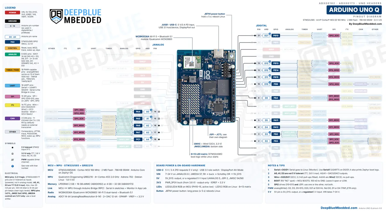
Arduino UNO Q Default SPI Pins: D11 (MOSI/COPI), D12 (MISO/CIPO), D13 (SCK), and D10 (SS).
| Signal | UNO Header | JSPI Pin | STM32 (UNO / JSPI) |
|---|---|---|---|
| SCK | D13 | 3 | PB13 / PD1 |
| MISO (CIPO) | D12 | 1 | PB14 / PC2 |
| MOSI (COPI) | D11 | 4 | PB15 / PC3 |
| SS (CS) | D10 | – | PB9 / none |
| 5V, RESET, GND | – | 2, 5, 6 | 5V_SYS, MCU NRST, GND |
Both sets of pins belong to the same SPI2 peripheral, so use either the UNO pins or JSPI, not both (Arduino’s pinout makes the same point). JSPI has no chip-select pin: pick any free GPIO for CS. The core’s second SPI object, SPI1, is SPI3, the internal link to Linux, so leave it alone.
There are so many modules that we can interface with the SPI bus, which include: TFT displays (ILI9341, ST7789), SD card modules, LoRa radios, nRF24L01 radios, MAX7219 LED drivers, W5500 Ethernet modules, and much more.
Arduino UNO Q CAN Pins
The Arduino UNO Q has 1 CAN FD controller (STM32 FDCAN1). Its default pins are D4 (CAN TX, PA12) and D5 (CAN RX, PA11). The board has no CAN transceiver, so you need an external one. The CAN pins are highlighted in purple in the pinout diagram.
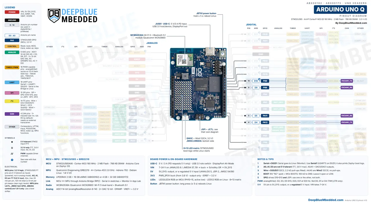
Arduino UNO Q Default CAN Pins: D4 (TX) and D5 (RX).
Since the board is 3.3v, use a 3.3v CAN transceiver like the SN65HVD230. Wire its TXD to D4 and RXD to D5, and terminate the bus with 120Ω at both ends. FDCAN1 can also be routed to D10 (TX) / D9 (RX) in the STM32, but the core uses D4/D5.
Arduino UNO Q USB-C Port
The Arduino UNO Q’s USB-C port belongs to the QRB2210, not to the STM32U585. It’s a USB 3.1 port with role switching: the board can be a USB device (to your PC, for App Lab) or a USB host (for a hub with a keyboard, mouse, and display, so it works as a standalone computer). It also outputs DisplayPort Alt-Mode video through the ANX7625 bridge, up to Full HD.
| Feature | Details |
|---|---|
| Power in | 5v, up to 3A (PD requests 5v/3A only) |
| Data | USB 3.1, host or device (role switching) |
| Video | DisplayPort Alt-Mode via ANX7625 (MIPI-DSI to DP); 1920×1080 max, 1280×720 recommended |
| Shared with | JMEDIA MIPI-DSI: only one display output is active at a time |
The STM32U585’s own USB pins (PA11/PA12) are used as D5/D4 on the UNO header, so the microcontroller has no USB of its own. Your sketch reaches the PC through Linux and the Bridge.
Arduino UNO Q BOOT, Reset and Debug Pins
The Arduino UNO Q has a BOOT pin (JANALOG 1) and a RESET pin (JANALOG 3, also JSPI 5) for the STM32U585, and the JCTL header for the QRB2210: its Linux console UART, its USB boot strap, and its volume keys. All JCTL pins are 1.8v.
| Pin | Where | Role | Notes |
|---|---|---|---|
| BOOT | JANALOG 1 | STM32 BOOT0 | 100kΩ pull-down; HIGH at reset = ST system bootloader |
| RESET | JANALOG 3, JSPI 5 | STM32 NRST, active LOW | Resets the MCU only; Linux keeps running |
| SWO / NJTRST | D2 / D8 | MCU trace / JTAG functions | Alternate functions only; SWD is wired to the QRB2210 |
Arduino UNO Q JCTL Header Pins
| Pin | Name | QRB2210 Pin | Function | Logic Level |
|---|---|---|---|---|
| 1 | GND | – | – | – |
| 2 | USB_BOOT | GPIO_95 | FORCED_USB_BOOT | 1.8v only |
| 3 | VOL_DOWN | GPIO_36 | VOL_DOWN key | 1.8v only |
| 4 | SE4_TX | GPIO_12 | SE4 UART_TX | 1.8v only |
| 5 | VOL_UP | GPIO_96 | VOL_UP key | 1.8v only |
| 6 | SE4_RX | GPIO_13 | SE4 UART_RX | 1.8v only |
| 7 | GND | – | – | – |
| 8 | PMIC_RST | – | PM4125 RESIN_N, active low | 1.8v |
| 9 | +1V8 | – | 1.8v out (L15A) | – |
| 10 | VBUS_DIS | – | USB VBUS switch off, active low | 1.8v |
- Linux console: JCTL 4 (TX) and 6 (RX), 115200 bps, 1.8v. Use a 1.8v USB-to-TTL adapter; a 3.3v or 5v adapter can damage the QRB2210.
- USB_BOOT (JCTL 2): held LOW at power-up, it forces the QRB2210 into USB download mode, which Arduino uses to re-flash the Linux image. The MCU can read its state (PG15).
- VOL_UP / VOL_DOWN (JCTL 5, 3): QRB2210 GPIOs used as volume keys.
- PMIC_RST and VBUS_DIS (JCTL 8, 10): Arduino describes them only as “PM4125 reset” and “VBUS power switch disable”, and the schematic notes the reset input as not defined, so leave them unconnected.
The STM32U585 has no SWD header: its SWD pins go to the QRB2210, and Linux flashes every sketch through them (OpenOCD). The BOOT pin is a recovery path only, since normal uploads never use the ST bootloader.
Arduino UNO Q JMISC & JMEDIA Pins (Camera, Display, Audio)
The Arduino UNO Q has two 60-pin, 1.27mm connectors on the bottom side for carrier boards. JMISC mixes 25 STM32U585 pins (3.3v), QRB2210 GPIO (1.8v), and the analog audio of the PM4125 codec (headphone, earpiece, line out, microphone). JMEDIA carries the QRB2210’s 2 MIPI-CSI camera ports (4 + 4 lanes), the MIPI-DSI display port (4 lanes), and the camera I2C and clock pins.
Arduino UNO Q JMISC Pins
Click to expand the full pin table (60 pins)
| Pin | Name | MCU / MPU Pin (Arduino #) | Functions | Logic Level |
|---|---|---|---|---|
| 1 | PSSI_D0 | PC6 (25) | TIM3_CH1, TIM8_CH1, DCMI_D0, SDMMC1_D6 | 5v tolerant |
| 2 | SDMMC1_CMD | PD2 (26) | UART5_RX, USART3_RTS, TRACED2, TIM3_ETR | 5v tolerant |
| 3 | PSSI_D1 | PC7 (27) | TIM3_CH2, TIM8_CH2, DCMI_D1, SDMMC1_D7 | 5v tolerant |
| 4 | TRACE_CLK | PE2 (28) | TRACECLK, TIM3_ETR | 5v tolerant |
| 5 | PSSI_D2 | PC8 (29) | TIM3_CH3, TIM8_CH3, DCMI_D2, SDMMC1_D0 | 5v tolerant |
| 6 | TRACE_D0 | PE3 (30) | TIM3_CH1, TRACED0 | 5v tolerant |
| 7 | PSSI_D3 | PC9 (31) | TIM3_CH4, TIM8_CH4, DCMI_D3, SDMMC1_D1 | 5v tolerant |
| 8 | TRACE_D2 | PE5 (32) | TIM3_CH3, TRACED2, DCMI_D6 | 5v tolerant |
| 9 | PSSI_D4 | PE4 (33) | TIM3_CH2, DCMI_D4, TRACED1 | 5v tolerant |
| 10 | TRACE_D3 | PE6 (34) | TIM3_CH4, TRACED3, DCMI_D7 | 5v tolerant |
| 11 | PSSI_D5 | PI4 (35) | DCMI_D5, TIM8_BKIN | 5v tolerant |
| 12 | PE7 | PE7 (36) | TIM1_ETR, WKUP6 | 5v tolerant |
| 13 | PSSI_D6 | PI6 (37) | TIM8_CH2, DCMI_D6 | 5v tolerant |
| 14 | PE8 | PE8 (38) | TIM1_CH1N, WKUP7 | 5v tolerant |
| 15 | PSSI_D7 | PI7 (39) | TIM8_CH3, DCMI_D7 | 5v tolerant |
| 16 | I2C4_SCL | PF14 (40) | ADC4_IN5, I2C4_SCL | 5v tolerant |
| 17 | PSSI_PDCK | PD9 (41) | USART3_RX, DCMI_PIXCLK | 5v tolerant |
| 18 | I2C4_SDA | PF15 (42) | ADC4_IN6, I2C4_SDA | 5v tolerant |
| 19 | PSSI_RDY | PI5 (43) | TIM8_CH1, DCMI_VSYNC | 5v tolerant |
| 20 | OPAMP1_OUT | PA3 (44) | OPAMP1_VOUT, ADC1_IN8, TIM2_CH4, TIM15_CH2, USART2_RX, LPUART1_RX | 3.3v only (3.6v max) |
| 21 | PSSI_DE | PD8 (45) | USART3_TX, DCMI_HSYNC | 5v tolerant |
| 22 | OPAMP1_INP | PA0 (46) | OPAMP1_VINP, ADC1_IN5, TIM2_CH1, TIM5_CH1, USART2_CTS, UART4_TX | 5v tolerant |
| 23 | MCO | PA8 (47) | TIM1_CH1, USART1_CK, MCO 12 MHz, TRACECLK | 5v tolerant |
| 24 | OPAMP1_INM | PA1 (48) | OPAMP1_VINM, ADC1_IN6, TIM2_CH2, TIM5_CH2, USART2_RTS, UART4_RX | 5v tolerant |
| 25 | CRS_SYNC | PA10 (49) | TIM1_CH3, USART1_RX, CRS_SYNC | 5v tolerant |
| 26 | GND | – | – | – |
| 27 | GND | – | – | – |
| 28 | EAR_P_R | – | Earpiece + | – |
| 29 | MIC2_INP | – | Mic 2 in+ | – |
| 30 | EAR_M_R | – | Earpiece − | – |
| 31 | MIC2_INM | – | Mic 2 in− | – |
| 32 | LINEOUT_P | – | Line out + | – |
| 33 | MIC2_BIAS | – | Mic 2 bias | – |
| 34 | LINEOUT_M | – | Line out − | – |
| 35 | GND | – | – | – |
| 36 | HPH_L | – | Headphone L | – |
| 37 | SOC_GPIO_0_SE0 | GPIO_0 | SE0 UART_CTS, SE0 SPI_MISO, SE0 I2C_SDA | 1.8v only |
| 38 | HPH_R | – | Headphone R | – |
| 39 | SOC_GPIO_1_SE0 | GPIO_1 | SE0 UART_RFR, SE0 SPI_MOSI, SE0 I2C_SCL | 1.8v only |
| 40 | HPH_REF | – | Headphone ref | – |
| 41 | SOC_GPIO_2_SE0 | GPIO_2 | SE0 UART_TX, SE0 SPI_SCLK | 1.8v only |
| 42 | HS_DET | – | Headset detect | – |
| 43 | SOC_GPIO_3_SE0 | GPIO_3 | SE0 UART_RX, SE0 SPI_CS0 | 1.8v only |
| 44 | GND | – | – | – |
| 45 | SOC_GPIO_86_SE0 | GPIO_86 | SE0 SPI_CS2 | 1.8v only |
| 46 | SOC_GPIO_98 | GPIO_98 | MI2S0_CLK, DMIC1_CLK | 1.8v only |
| 47 | SOC_GPIO_82_SE0 | GPIO_82 | PWM[6], SE0 SPI_CS1 | 1.8v only |
| 48 | SOC_GPIO_99 | GPIO_99 | MI2S0_WS, DMIC1_DATA | 1.8v only |
| 49 | SOC_GPIO_18 | GPIO_18 | PWM[0] | 1.8v only |
| 50 | SOC_GPIO_100 | GPIO_100 | MI2S0_DATA0, DMIC2_CLK | 1.8v only |
| 51 | SOC_GPIO_28 | GPIO_28 | CAM_MCLK3 | 1.8v only |
| 52 | SOC_GPIO_101 | GPIO_101 | MI2S0_DATA1, DMIC2_DATA | 1.8v only |
| 53 | +3V3 | – | 3.3v out | – |
| 54 | +5V | – | 5V_SYS in/out | – |
| 55 | +3V3 | – | 3.3v out | – |
| 56 | +5V | – | 5V_SYS in/out | – |
| 57 | +1V8 | – | 1.8v out (L15A) | – |
| 58 | GND | – | – | – |
| 59 | VCOIN | – | RTC coin cell in | – |
| 60 | VBAT | – | 3.8v rail (reserved) | – |
Arduino UNO Q JMEDIA Pins
Click to expand the full pin table (60 pins)
| Pin | Name | MPU Pin | Functions | Logic Level |
|---|---|---|---|---|
| 1 | GND | – | – | – |
| 2 | GND | – | – | – |
| 3 | DSI0_CLK_M | – | DSI clock − | – |
| 4 | DSI0_L1_P | – | DSI lane 1 + | – |
| 5 | DSI0_CLK_P | – | DSI clock + | – |
| 6 | DSI0_L1_M | – | DSI lane 1 − | – |
| 7 | GND | – | – | – |
| 8 | GND | – | – | – |
| 9 | DSI0_L2_M | – | DSI lane 2 − | – |
| 10 | DSI0_L0_P | – | DSI lane 0 + | – |
| 11 | DSI0_L2_P | – | DSI lane 2 + | – |
| 12 | DSI0_L0_M | – | DSI lane 0 − | – |
| 13 | GND | – | – | – |
| 14 | GND | – | – | – |
| 15 | DSI0_L3_M | – | DSI lane 3 − | – |
| 16 | CAM_MCLK0 | GPIO_20 | Camera clock 0 | 1.8v only |
| 17 | DSI0_L3_P | – | DSI lane 3 + | – |
| 18 | CAM_MCLK1 | GPIO_21 | Camera clock 1 | 1.8v only |
| 19 | GND | – | – | – |
| 20 | GND | – | – | – |
| 21 | CSI0_LN0_M | – | CSI0 data 0 − | – |
| 22 | CCI_SDA1 | GPIO_29 | CCI_I2C_SDA1 | 1.8v only |
| 23 | CSI0_LN0_P | – | CSI0 data 0 + | – |
| 24 | CCI_SCL1 | GPIO_30 | CCI_I2C_SCL1 | 1.8v only |
| 25 | GND | – | – | – |
| 26 | GND | – | – | – |
| 27 | CSI0_LN1_M | – | CSI0 data 1 − | – |
| 28 | CSI1_LN3_P | – | CSI1 data 3 + | – |
| 29 | CSI0_LN1_P | – | CSI0 data 1 + | – |
| 30 | CSI1_LN3_M | – | CSI1 data 3 − | – |
| 31 | GND | – | – | – |
| 32 | GND | – | – | – |
| 33 | CSI0_CLK_M | – | CSI0 clock − | – |
| 34 | CSI1_LN2_P | – | CSI1 data 2 + | – |
| 35 | CSI0_CLK_P | – | CSI0 clock + | – |
| 36 | CSI1_LN2_M | – | CSI1 data 2 − | – |
| 37 | GND | – | – | – |
| 38 | GND | – | – | – |
| 39 | CSI0_LN2_M | – | CSI0 data 2 − | – |
| 40 | CSI1_CLK_P | – | CSI1 clock + | – |
| 41 | CSI0_LN2_P | – | CSI0 data 2 + | – |
| 42 | CSI1_CLK_M | – | CSI1 clock − | – |
| 43 | GND | – | – | – |
| 44 | GND | – | – | – |
| 45 | CSI0_LN3_M | – | CSI0 data 3 − | – |
| 46 | CSI1_LN1_P | – | CSI1 data 1 + | – |
| 47 | CSI0_LN3_P | – | CSI0 data 3 + | – |
| 48 | CSI1_LN1_M | – | CSI1 data 1 − | – |
| 49 | GND | – | – | – |
| 50 | GND | – | – | – |
| 51 | CCI_SCL0 | GPIO_23 | CCI_I2C_SCL0 | 1.8v only |
| 52 | CSI1_LN0_P | – | CSI1 data 0 + | – |
| 53 | CCI_SDA0 | GPIO_22 | CCI_I2C_SDA0 | 1.8v only |
| 54 | CSI1_LN0_M | – | CSI1 data 0 − | – |
| 55 | GND | – | – | – |
| 56 | GND | – | – | – |
| 57 | VIN | – | 7v–24v in | – |
| 58 | +3V3 | – | 3.3v out | – |
| 59 | VIN | – | 7v–24v in | – |
| 60 | +3V3 | – | 3.3v out | – |
- JMISC 1–25: the STM32U585’s PSSI/DCMI parallel camera bus (D0–D7, PDCK, RDY, DE), trace pins, OPAMP1, I2C4, and the 12MHz MCO clock that the core enables on JMISC 23. They’re Arduino pins 25–49.
- JMISC 37–52: QRB2210 1.8v GPIO. The functions listed (SE0 UART/SPI/I2C, I2S, PWM, camera clock) come from Qualcomm’s data sheet; which ones Arduino’s Linux image actually enables is not documented, so check the device tree before you rely on one.
- JMEDIA: MIPI lanes are high-speed differential pairs. A carrier board needs matched, impedance-controlled routing. And the DSI port is shared with USB-C DisplayPort: one display at a time.
Arduino UNO Q On-Board Features
Besides the connectors, the Arduino UNO Q has an 8×13 LED matrix, four RGB LEDs, a power LED, and a power button. Here’s what each one does and which processor drives it.
| Part | Driven By | What It Does |
|---|---|---|
| LED matrix (8×13, blue) | STM32U585 (PF0–PF10) | Shows the boot logo while Linux starts, then the graphics your sketch draws |
| RGB LED3 | STM32U585 (PH10–PH12, active LOW) | LED_BUILTIN (red) and the core’s error LED |
| RGB LED4 | STM32U585 (PH13–PH15, active LOW) | User LED for your sketch |
| RGB LED1 | QRB2210 | User LED for Linux (/sys/class/leds) |
| RGB LED2 | QRB2210 | Linux status: red = panic, green = Wi-Fi, blue = Bluetooth |
| Power LED (ON) | 3.3v rail | On whenever the board is powered |
| Power button (JBTN1) | PM4125 PMIC | Press and hold for 5 seconds or more to reboot Linux |
A note on the LED matrix: it shows the boot animation for about 20–30 seconds while Linux starts. Arduino’s datasheet warns that driving it before then can interfere, so wait for the boot to finish before your sketch takes over the matrix.
Getting Started With Arduino UNO Q
You program the Arduino UNO Q with Arduino App Lab, which runs on your PC or directly on the board (with a USB-C hub, keyboard, mouse, and display). An App combines an Arduino sketch for the STM32U585, Python code for Linux, and optional machine-learning models, and App Lab builds and flashes both sides for you.
- Arduino App Lab: connect the board over USB-C (or Wi-Fi after setup), create an App, and write the sketch and the Python side together. The first boot takes about 20–30 seconds.
- Arduino IDE 2: install the UNO Q board package (Arduino’s Zephyr-based core) from the Boards Manager to write sketches for the STM32U585 only.
- Library choice: the core is Zephyr-based, not the classic AVR core, so libraries that touch AVR registers won’t compile. Arduino APIs ( digitalWrite, Wire, SPI, Serial) work as usual.
| Arduino Name | Pin | Default |
|---|---|---|
Serial | Bridge (no pin) | App Lab console on Linux |
Serial1 | D0 (RX), D1 (TX) | USART1 |
Serial3 | D20 (RX), D21 (TX) | USART3 |
Wire | D20 (SDA), D21 (SCL) | I2C2, 2.2kΩ pull-ups |
Wire1 | Qwiic connector | I2C4 |
Wire2 | A4 (SDA), A5 (SCL) | I2C3, no pull-ups |
SPI | D11 / D12 / D13, SS = D10 | SPI2 (also on JSPI) |
DAC0 / DAC1 | A0 / A1 | 12-bit DAC |
LED_BUILTIN | RGB LED3 red (PH10) | Active LOW (handled by the core) |
Arduino UNO Q Common Problems & Fixes
Why doesn’t Serial.print() show anything on D0/D1? Because Serial on the UNO Q goes to Linux and the App Lab console, not to D0/D1. Use Serial1 for the D0/D1 pins (Arduino Forum).
Why does text appear on D1 when the board resets? That’s the Zephyr OS boot log on USART1 ( Serial1). It happens after every MCU reset; let your module ignore it.
Why isn’t my Qwiic sensor found? The Qwiic port is Wire1. Call Wire1.begin() and pass Wire1 to the sensor library.
Why doesn’t my I2C shield on A4/A5 work? On the UNO Q, A4/A5 are Wire2 (I2C3) with no pull-ups, and the SDA/SCL pins are a different bus ( Wire). Use Wire2 and add pull-ups, or rewire the shield to D20/D21.
Can I connect a 5v sensor directly? Only to 5v-tolerant digital inputs, and never to A0, A1, or D3. The UNO Q’s outputs are 3.3v, so a 5v module may not read them as HIGH: use a level shifter.
Why does my 5v shield not work? Shields that expect 5v logic or check IOREF see 3.3v here. Check the shield’s logic level; many 3.3v-ready shields work, 5v-only ones don’t.
Why is the LED matrix showing the logo instead of my sketch? Linux is still booting (about 20–30 seconds). Wait for the boot to finish.
Why do I see garbage on the Linux console? JCTL is 1.8v at 115200 bps. A 3.3v adapter can misread it and can damage the QRB2210; use a 1.8v USB-to-TTL adapter.
Arduino UNO Q vs UNO R4 WiFi vs UNO R3
The Arduino UNO Q keeps the UNO shape and header positions, but it’s a Linux computer plus a 3.3v microcontroller. Here’s how it compares with the UNO R4 WiFi and the classic UNO R3:
| Feature | Arduino UNO Q | Arduino UNO R4 WiFi | Arduino UNO R3 |
|---|---|---|---|
| Main chip(s) | QRB2210 (Linux) + STM32U585 | Renesas RA4M1 + ESP32-S3 (Wi-Fi) | ATmega328P |
| MCU clock | 160MHz Cortex-M33 | 48MHz Cortex-M4F | 16MHz AVR |
| MCU flash / RAM | 2MB / 786KB | 256KB / 32KB | 32KB / 2KB |
| Linux / RAM / storage | Debian, 2GB or 4GB, 16GB or 32GB eMMC | No | No |
| Logic level | 3.3v (most pins 5v-tolerant inputs) | 5v | 5v |
| ADC | 6 pins, up to 14-bit | 6 pins, up to 14-bit | 6 pins, 10-bit |
| DAC | 2 (A0, A1) | 1 (A0) | No |
| I2C on A4/A5 | Separate bus (Wire2); Wire is SDA/SCL | Same pins as SDA/SCL | Same pins as SDA/SCL |
| Wireless | Wi-Fi 5 dual-band, Bluetooth 5.1 | Wi-Fi 4, Bluetooth LE 5 | No |
| LED matrix | 8×13 blue | 12×8 red | No |
| Qwiic | Yes (Wire1) | Yes (Wire1) | No |
| CAN | Yes (FDCAN, D4/D5) | Yes (D4/D5) | No |
| USB | USB-C 3.1, host/device, DisplayPort out | USB-C | USB-B |
| VIN range | 7v–24v | 6v–24v | 7v–12v recommended |
| Camera / display / audio | Yes (JMEDIA, JMISC) | No | No |
Pick the Arduino UNO Q when your project needs Linux next to real-time I/O: a camera with machine vision, a web dashboard, Python, or a display, plus sensors and motors on the UNO pins. Pick the UNO R4 WiFi when you want a simple 5v Arduino with Wi-Fi and full compatibility with 5v shields. And the classic UNO R3 is still the simplest 5v board to learn on; see my Arduino UNO pinout guide for its pins.
Arduino UNO Q Pin Details
Here is every Arduino UNO Q UNO header pin in physical order, with its Arduino number, STM32U585 pin, main functions, all its alternate functions from ST’s pin data, its 5v tolerance, and a short description. With the USB-C connector at the top, JANALOG is the left header, numbered from the top (pin 1 = BOOT), and JDIGITAL is the right header, numbered from the bottom (pin 1 = D0). The JCTL, JMISC, and JMEDIA tables are in their own sections above.
Arduino UNO Q JANALOG Header Pins
Click to expand the full pin table (14 pins)
| Pin | Label | Arduino # | STM32 Pin | Main Functions | All Alternate Functions | 5v Tolerant | Description |
|---|---|---|---|---|---|---|---|
| JANALOG 1 | BOOT | – | – | MCU BOOT0 (100kΩ pull-down) | – | – | The STM32U585 BOOT0 pin (100kΩ pull-down). Leave it open; pulled HIGH at reset, it starts ST’s system bootloader instead of your sketch. |
| JANALOG 2 | IOREF | – | – | 3.3v out | – | – | Tells shields the logic level of this board: 3.3v (it’s tied to the 3.3v rail). |
| JANALOG 3 | RESET | – | – | MCU NRST (2.2kΩ pull-up) | – | – | Resets the STM32U585 only (active LOW, 2.2kΩ pull-up); Linux on the QRB2210 keeps running. |
| JANALOG 4 | 3V3 | – | – | 3.3v out | – | – | 3.3v output of the board’s buck regulator; output only. |
| JANALOG 5 | 5V | – | – | 5V_SYS in/out | – | – | The 5V_SYS rail: a 5v output when the board runs from USB-C or VIN, or a regulated 5v input. |
| JANALOG 6 | GND | – | – | – | – | – | Ground. |
| JANALOG 7 | GND | – | – | – | – | – | Ground. |
| JANALOG 8 | VIN | – | – | 7v–24v in | – | – | External supply input, 7v to 24v, into the 5v buck converter. |
| JANALOG 9 | A0 | 14 | PA4 | ADC1_IN9, DAC1_OUT1, USART2_CK, SPI1_NSS, SPI3_NSS, LPTIM2_CH1 | ADC1_IN9, ADC4_IN9, DAC1_OUT1, DCMI_HSYNC, LPTIM2_CH1, OCTOSPIM_P1_NCS, PSSI_DE, PWR_WKUP2, SAI1_FS_B, SPI1_NSS, SPI3_NSS, USART2_CK | 3.3v only (3.6v max) | Analog input and the 12-bit DAC0 output; not 5v tolerant (3.6v max). |
| JANALOG 10 | A1 | 15 | PA5 | ADC1_IN10, DAC1_OUT2, TIM2_CH1, TIM8_CH1N, USART3_RX, SPI1_SCK, LPTIM2_ETR | ADC1_IN10, ADC4_IN10, DAC1_OUT2, LPTIM2_ETR, PSSI_D14, PWR_CSLEEP, PWR_WKUP6, SPI1_SCK, TIM2_CH1, TIM2_ETR, TIM8_CH1N, USART3_RX | 3.3v only (3.6v max) | Analog input and the 12-bit DAC1 output; not 5v tolerant (3.6v max). |
| JANALOG 11 | A2 | 16 | PA6 | ADC1_IN11, OPAMP2_VINP, TIM3_CH1, TIM16_CH1, USART3_CTS, LPUART1_CTS, SPI1_MISO | ADC1_IN11, ADC4_IN11, DCMI_PIXCLK, LPUART1_CTS, OCTOSPIM_P1_IO3, OPAMP2_VINP, PSSI_PDCK, PWR_CDSTOP, PWR_WKUP7, SPI1_MISO, TIM16_CH1, TIM1_BKIN, TIM3_CH1, TIM8_BKIN, USART3_CTS | 5v tolerant | Analog input (ADC1 channel 11); 5v tolerant only in digital mode. |
| JANALOG 12 | A3 | 17 | PA7 | ADC1_IN12, OPAMP2_VINM, TIM3_CH2, TIM17_CH1, USART3_TX, SPI1_MOSI, I2C3_SCL | ADC1_IN12, ADC4_IN20, I2C3_SCL, LPTIM2_CH2, OCTOSPIM_P1_IO2, OPAMP2_VINM, PWR_SRDSTOP, PWR_WKUP8, SPI1_MOSI, TIM17_CH1, TIM1_CH1N, TIM3_CH2, TIM8_CH1N, USART3_TX | 5v tolerant | Analog input (ADC1 channel 12); 5v tolerant only in digital mode. |
| JANALOG 13 | A4 | 18 | PC1 | ADC1_IN2, LPUART1_TX, SPI2_MOSI, I2C3_SDA, LPTIM1_CH1 | ADC1_IN2, ADC4_IN2, DEBUG_TRACED0, I2C3_SDA, LPTIM1_CH1, LPUART1_TX, MDF1_CKI4, OCTOSPIM_P1_IO4, SAI1_SD_A, SDMMC2_CK, SPI2_MOSI | 5v tolerant | Analog input and the SDA pin of Wire2 (I2C3), not of Wire like on the UNO R3. |
| JANALOG 14 | A5 | 19 | PC0 | ADC1_IN1, LPUART1_RX, I2C3_SCL, LPTIM1_IN1 | ADC1_IN1, ADC4_IN1, I2C3_SCL, LPTIM1_IN1, LPTIM2_IN1, LPUART1_RX, MDF1_SDI4, OCTOSPIM_P1_IO7, SAI2_FS_A, SDMMC1_D5, SPI2_RDY | 5v tolerant | Analog input and the SCL pin of Wire2 (I2C3), not of Wire like on the UNO R3. |
Arduino UNO Q JDIGITAL Header Pins
Click to expand the full pin table (18 pins)
| Pin | Label | Arduino # | STM32 Pin | Main Functions | All Alternate Functions | 5v Tolerant | Description |
|---|---|---|---|---|---|---|---|
| JDIGITAL 1 | D0 | 0 | PB7 | TIM4_CH2, TIM17_CH1N, USART1_RX, I2C1_SDA, I2C4_SDA, WKUP4 | COMP2_INM, DCMI_VSYNC, FMC_NL, I2C1_SDA, I2C4_SDA, LPTIM1_IN2, MDF1_CKI5, PSSI_RDY, PWR_PVD_IN, PWR_WKUP4, TIM17_CH1N, TIM4_CH2, TIM8_BKIN, TSC_G2_IO4, UART4_CTS, USART1_RX | 5v tolerant | Serial1 RX (USART1); Zephyr also prints its boot messages on this UART. |
| JDIGITAL 2 | D1 | 1 | PB6 | TIM4_CH1, TIM16_CH1N, USART1_TX, I2C1_SCL, I2C4_SCL, WKUP3 | COMP2_INP, DCMI_D5, I2C1_SCL, I2C4_SCL, LPTIM1_ETR, MDF1_SDI5, PSSI_D5, PWR_WKUP3, SAI1_FS_B, TIM16_CH1N, TIM4_CH1, TIM8_BKIN2, TSC_G2_IO3, USART1_TX | 5v tolerant | Serial1 TX (USART1); expect the Zephyr boot banner here after every MCU reset. |
| JDIGITAL 3 | D2 | 2 | PB3 | TIM2_CH2, USART1_RTS, SPI1_SCK, SPI3_SCK, I2C1_SDA, SWO, CRS_SYNC | ADF1_CCK0, COMP2_INM, CRS_SYNC, DEBUG_JTDO-SWO, I2C1_SDA, LPTIM1_CH1, SAI1_SCK_B, SDMMC2_D2, SPI1_SCK, SPI3_SCK, TIM2_CH2, USART1_DE, USART1_RTS | 5v tolerant | General I/O and a PWM pin (TIM2_CH2); also the SWO trace pin. |
| JDIGITAL 4 | D3 | 3 | PB0 | ADC1_IN15, OPAMP2_VOUT, TIM3_CH3, TIM1_CH2N, USART3_CK, SPI1_NSS, COMP1_OUT | ADC1_IN15, ADC4_IN18, AUDIOCLK, COMP1_OUT, LPTIM3_CH1, OCTOSPIM_P1_IO1, OPAMP2_VOUT, SPI1_NSS, TIM1_CH2N, TIM3_CH3, TIM8_CH2N, USART3_CK | 3.3v only (3.6v max) | PWM pin (TIM3_CH3), and the only UNO digital pin that is not 5v tolerant (3.6v max). |
| JDIGITAL 5 | D4 | 4 | PA12 | TIM1_ETR, USART1_RTS, SPI1_MOSI, FDCAN1_TX | FDCAN1_TX, OCTOSPIM_P2_NCS, SPI1_MOSI, TIM1_ETR, USART1_DE, USART1_RTS, USB_OTG_FS_DP | 5v tolerant | The CAN TX pin (FDCAN1); no PWM on this pin. |
| JDIGITAL 6 | D5 | 5 | PA11 | TIM1_CH4, USART1_CTS, SPI1_MISO, FDCAN1_RX | ADC1_EXTI11, FDCAN1_RX, SPI1_MISO, TIM1_BKIN2, TIM1_CH4, USART1_CTS, USB_OTG_FS_DM | 5v tolerant | The CAN RX pin (FDCAN1) and a PWM pin (TIM1_CH4). |
| JDIGITAL 7 | D6 | 6 | PB1 | ADC1_IN16, TIM3_CH4, TIM1_CH3N, USART3_RTS, LPUART1_RTS, LPTIM2_IN1 | ADC1_IN16, ADC4_IN19, COMP1_INM, LPTIM2_IN1, LPTIM3_CH2, LPUART1_DE, LPUART1_RTS, MDF1_SDI0, OCTOSPIM_P1_IO0, PWR_WKUP4, TIM1_CH3N, TIM3_CH4, TIM8_CH3N, USART3_DE, USART3_RTS | 5v tolerant | PWM pin (TIM3_CH4) with no other default role. |
| JDIGITAL 8 | D7 | 7 | PB2 | ADC1_IN17, TIM8_CH4N, I2C3_SMBA, LPTIM1_CH1, RTC_OUT2 | ADC1_IN17, COMP1_INP, I2C3_SMBA, LPTIM1_CH1, MDF1_CKI0, OCTOSPIM_P1_DQS, PWR_WKUP1, RTC_OUT2, SPI1_RDY, TIM8_CH4N, UCPD1_FRSTX1 | 5v tolerant | PWM pin (TIM8_CH4N, a complementary channel). |
| JDIGITAL 9 | D8 | 8 | PB4 | TIM3_CH1, USART1_CTS, SPI1_MISO, SPI3_MISO, I2C3_SDA, NJTRST | ADF1_SDI0, COMP2_INP, DCMI_D12, DEBUG_NJTRST, I2C3_SDA, LPTIM1_CH2, PSSI_D12, SAI1_MCLK_B, SDMMC2_D3, SPI1_MISO, SPI3_MISO, TIM17_BKIN, TIM3_CH1, TSC_G2_IO1, UART5_DE, UART5_RTS, USART1_CTS | 5v tolerant | PWM pin (TIM3_CH1); also the JTAG NJTRST pin of the MCU. |
| JDIGITAL 10 | D9 | 9 | PB8 | TIM4_CH3, TIM16_CH1, I2C1_SCL, FDCAN1_RX | DCMI_D6, FDCAN1_RX, I2C1_SCL, MDF1_CCK0, PSSI_D6, PWR_WKUP5, SAI1_CK1, SAI1_MCLK_A, SDMMC1_CKIN, SDMMC1_D4, SDMMC2_D4, SPI3_RDY, TIM16_CH1, TIM4_CH3 | 5v tolerant | PWM pin (TIM4_CH3) with no other default role. |
| JDIGITAL 11 | D10 | 10 | PB9 | TIM4_CH4, TIM17_CH1, SPI2_NSS, I2C1_SDA, FDCAN1_TX, IR_OUT | DAC1_EXTI9, DCMI_D7, FDCAN1_TX, I2C1_SDA, IR_OUT, PSSI_D7, SAI1_D2, SAI1_FS_A, SDMMC1_CDIR, SDMMC1_D5, SDMMC2_D5, SPI2_NSS, TIM17_CH1, TIM4_CH4 | 5v tolerant | The SPI SS (CS) pin and a PWM pin (TIM4_CH4). |
| JDIGITAL 12 | D11 | 11 | PB15 | TIM1_CH3N, TIM15_CH2, SPI2_MOSI, RTC_REFIN | ADC1_EXTI15, ADC4_EXTI15, FMC_NBL1, LPTIM2_IN2, MDF1_CKI2, PWR_WKUP7, RTC_REFIN, SAI2_SD_A, SDMMC2_D1, SPI2_MOSI, TIM15_CH2, TIM1_CH3N, TIM8_CH3N, UCPD1_CC2 | 5v tolerant | The SPI MOSI (COPI) pin and a PWM pin (TIM1_CH3N). |
| JDIGITAL 13 | D12 | 12 | PB14 | TIM1_CH2N, TIM15_CH1, USART3_RTS, SPI2_MISO, I2C2_SDA | I2C2_SDA, LPTIM3_ETR, MDF1_SDI2, SAI2_MCLK_A, SDMMC2_D0, SPI2_MISO, TIM15_CH1, TIM1_CH2N, TIM8_CH2N, TSC_G1_IO3, UCPD1_DBCC2, USART3_DE, USART3_RTS | 5v tolerant | The SPI MISO (CIPO) pin and a PWM pin (TIM1_CH2N). |
| JDIGITAL 14 | D13 | 13 | PB13 | TIM1_CH1N, TIM15_CH1N, USART3_CTS, LPUART1_CTS, SPI2_SCK, I2C2_SCL | I2C2_SCL, LPTIM3_IN1, LPUART1_CTS, MDF1_CKI1, SAI2_SCK_A, SPI2_SCK, TIM15_CH1N, TIM1_CH1N, TSC_G1_IO2, USART3_CTS | 5v tolerant | The SPI SCK pin and a PWM pin (TIM1_CH1N); there’s no LED on D13. |
| JDIGITAL 15 | GND | – | – | – | – | – | Ground. |
| JDIGITAL 16 | AREF | – | – | MCU VREF+ | – | – | The MCU’s VREF+ pin, for an external ADC reference (analogReference(AR_EXTERNAL)). |
| JDIGITAL 17 | D20 | 20 | PB11 | TIM2_CH4, USART3_RX, LPUART1_TX, I2C2_SDA, I2C4_SDA, COMP2_OUT | ADC1_EXTI11, COMP2_OUT, I2C2_SDA, I2C4_SDA, LPUART1_TX, OCTOSPIM_P1_NCS, SPI2_RDY, TIM2_CH4, USART3_RX | 5v tolerant | The SDA pin of Wire (I2C2, 2.2kΩ pull-up), and Serial3 RX (USART3). |
| JDIGITAL 18 | D21 | 21 | PB10 | TIM2_CH3, USART3_TX, LPUART1_RX, SPI2_SCK, I2C2_SCL, I2C4_SCL, COMP1_OUT | COMP1_OUT, I2C2_SCL, I2C4_SCL, LPTIM3_CH1, LPUART1_RX, OCTOSPIM_P1_CLK, PWR_WKUP8, SAI1_SCK_A, SPI2_SCK, TIM2_CH3, TSC_SYNC, USART3_TX | 5v tolerant | The SCL pin of Wire (I2C2, 2.2kΩ pull-up), and Serial3 TX (USART3). |
Arduino UNO Q JSPI & Qwiic Pins
Click to expand the full pin table (10 pins)
| Pin | Name | STM32 Pin (Arduino #) | Functions | 5v Tolerant |
|---|---|---|---|---|
| JSPI 1 | MISO | PC2 (22) | ADC1_IN3, SPI2_MISO | 5v tolerant |
| JSPI 2 | +5V | – | 5V_SYS in/out | – |
| JSPI 3 | SCK | PD1 (24) | SPI2_SCK, FDCAN1_TX | 5v tolerant |
| JSPI 4 | MOSI | PC3 (23) | ADC1_IN4, SPI2_MOSI | 5v tolerant |
| JSPI 5 | RESET | – | MCU NRST | – |
| JSPI 6 | GND | – | – | – |
| Qwiic 1 | GND | – | – | – |
| Qwiic 2 | 3V3 | – | 3.3v out | – |
| Qwiic 3 | SDA | PD13 | ADC4_IN17, I2C4_SDA | 5v tolerant |
| Qwiic 4 | SCL | PD12 | ADC4_IN16, I2C4_SCL | 5v tolerant |
Wrap Up
To conclude this guide article, the Arduino UNO Q is a very capable board that puts a Linux computer and a fast STM32 microcontroller in the familiar UNO shape. The STM32U585 owns the UNO headers, JSPI, and Qwiic at 3.3v; the QRB2210 owns USB-C, Wi-Fi, JCTL, and the camera, display, and audio pins at 1.8v. Just remember the board-level gotchas: A0, A1, and D3 aren’t 5v tolerant, Serial goes to Linux (use Serial1 on D0/D1), Wire is on D20/D21 while A4/A5 are Wire2, and Qwiic is Wire1.
I hope you’ve found this guide helpful or useful for your project. For more boards, check out the Pinouts, Datasheets & Schematic Diagrams Library. Follow this Arduino Series of Tutorials to learn more about Arduino programming.
If you’re just getting started with Arduino, you need to check out the Arduino Getting Started Ultimate Guide below.
The complete beginner’s guide to Arduino programming: installing the IDE, your first sketch, and the Arduino tutorials series step by step.
