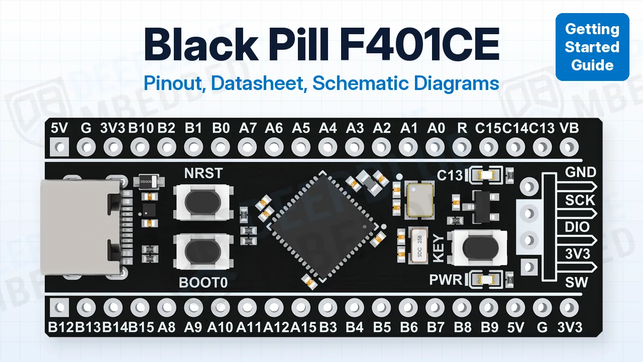
In this guide, you’ll find the Black Pill F401CE pinout diagram (both side headers and the SWD header), the datasheet and schematic, and every pin group explained with its default pins and gotchas. Without further ado, let’s get right into it!
The Black Pill F401CE is WeAct Studio’s “Black Pill” core board with the STM32F401CEU6, an 84MHz Arm Cortex-M4 with FPU, 512KB Flash and 96KB RAM. It packs 32 GPIO pins on two breadboard-friendly headers, a USB-C port wired to the MCU’s own USB, and a 25MHz crystal, on a board just 21mm wide.
Black Pill F401CE Pinout Diagram
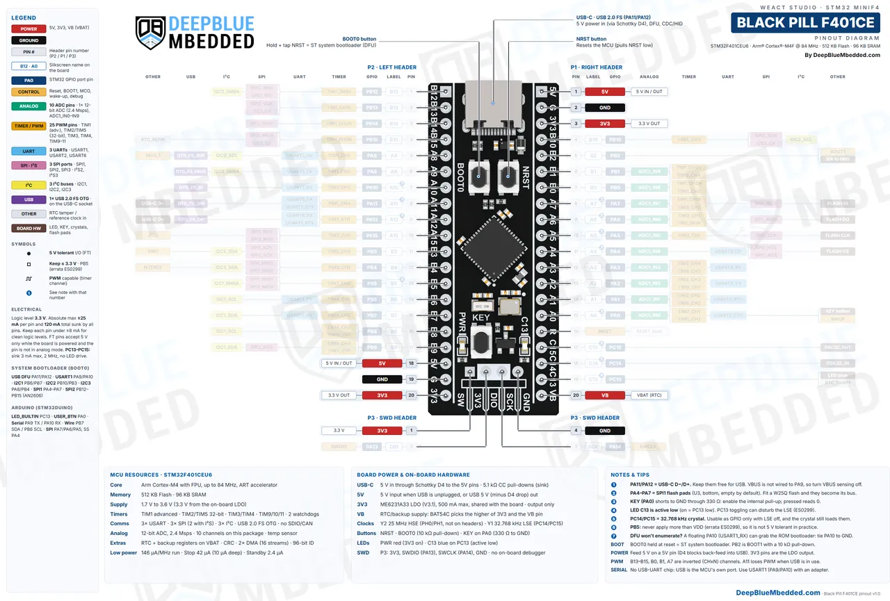
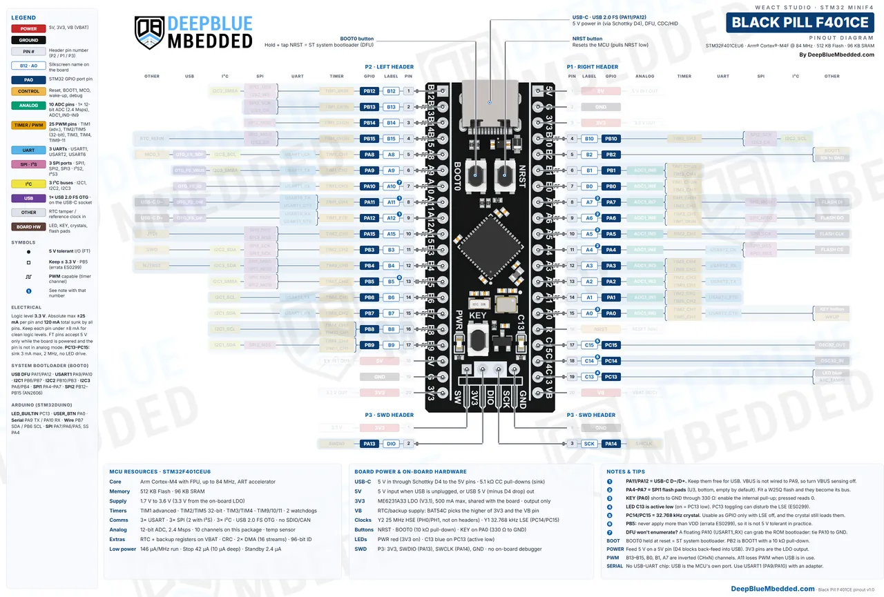
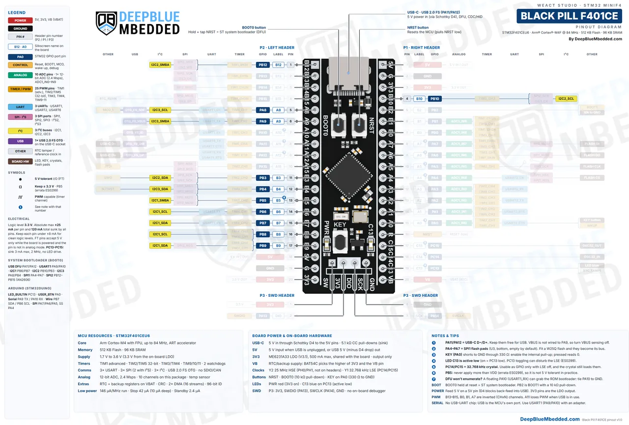
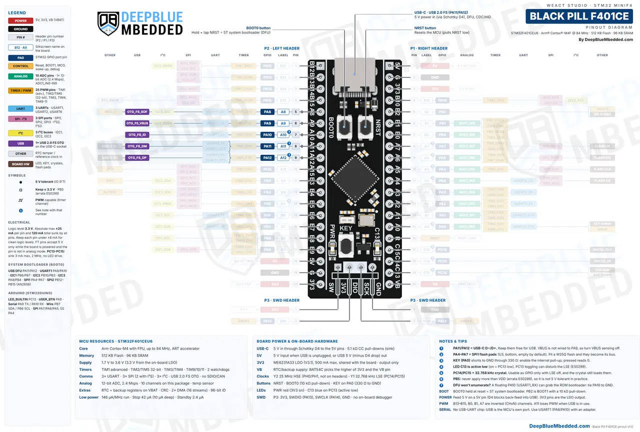
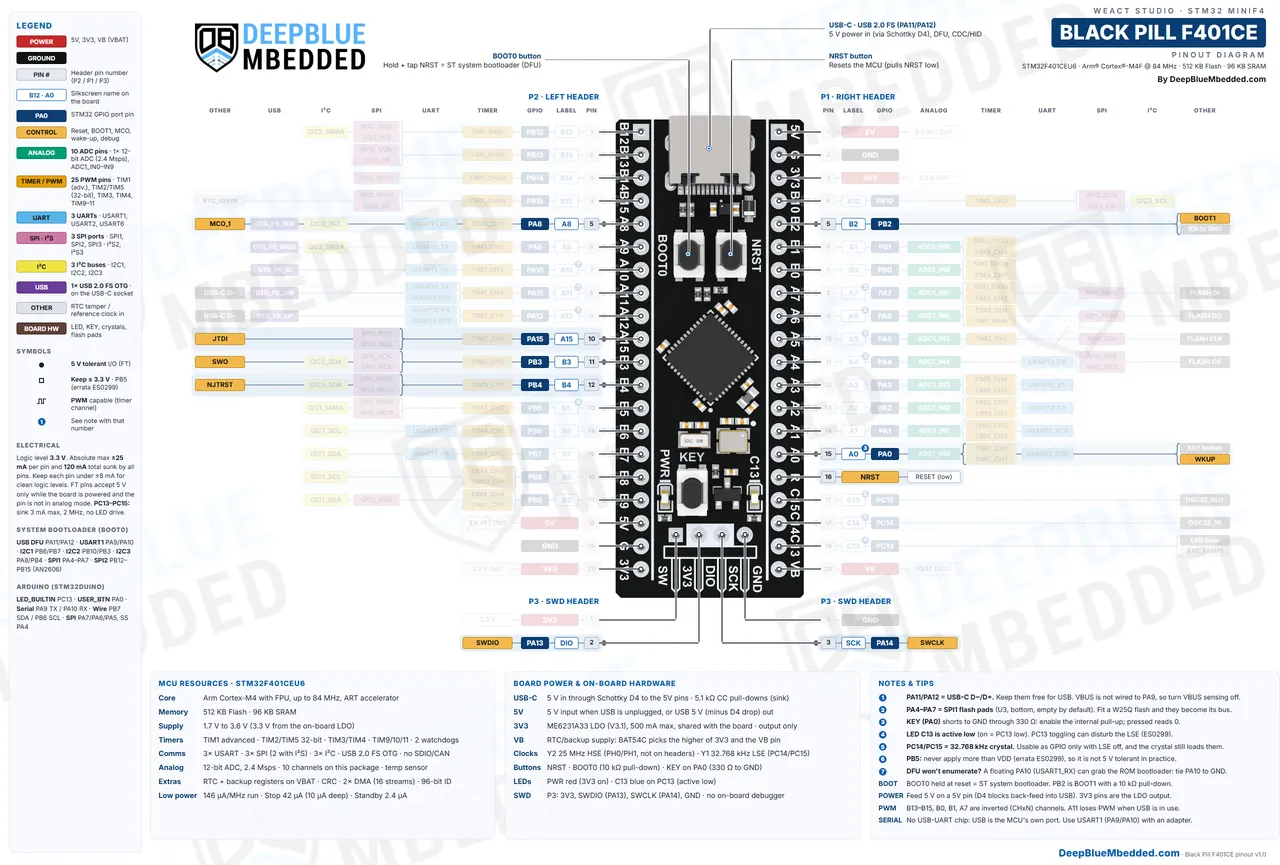
Here is a detailed Black Pill F401CE Pinout Diagram with colored labels and legends to help you easily identify the functionalities that each pin can perform. It covers both 20-pin side headers (P2 on the left, P1 on the right) and the 4-pin SWD header (P3) at the end of the board.
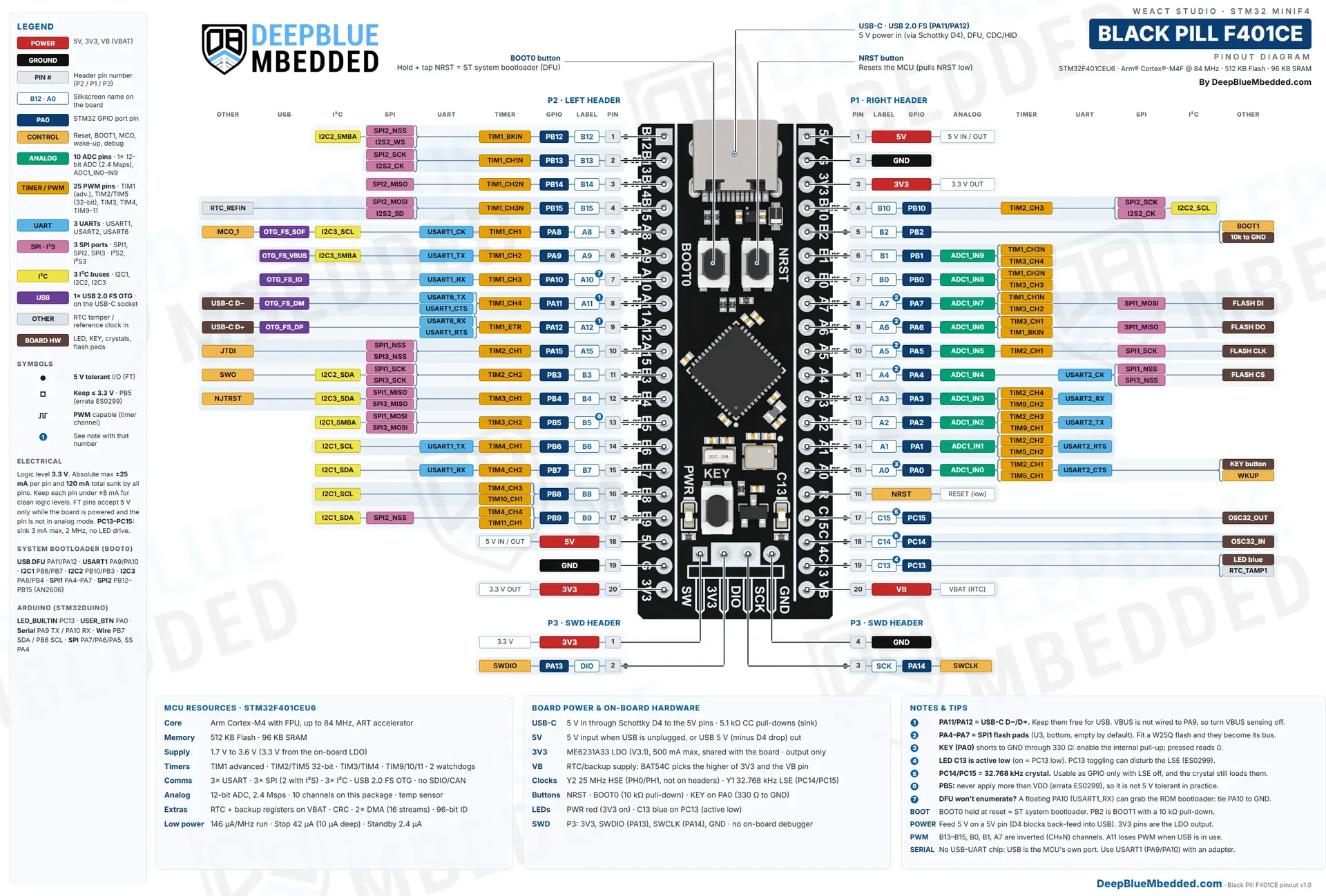
Each row shows the header pin number, the silkscreen label (B12, A8…), the STM32 GPIO name and its alternate functions, color-coded by peripheral. The small dot marks a 5v-tolerant pin, the square marks PB5 (keep it at 3.3v or below, see the errata note), and the numbered badges point to the notes at the bottom of the diagram.
Pin 1 of each header has a square pad. With the USB-C connector at the top, P2 (left) runs from B12 (pin 1) down to 3V3 (pin 20), and P1 (right) runs from 5V (pin 1) down to VB (pin 20). The two headers are 15.24mm (600 mil) apart, so the board fits a standard breadboard.
Buy an STM32F401 Black Pill: If you don’t have one yet, you can get one from Amazon or AliExpress. WeAct has discontinued the F401CE, so most F401 boards sold today carry the STM32F401CCU6, which has the same pinout with 256KB of Flash.
Download Black Pill F401CE Pinout Diagram (Full Resolution)
The Black Pill F401CE pinout diagram (P1, P2 and SWD headers) in full resolution (5120×3460 px WebP), in one ZIP file. Print it, zoom in, or keep it next to your bench. Please consider supporting my work if it helped you.
Black Pill F401CE Datasheet
This development board is built around the STM32F401CEU6 microcontroller (UFQFPN48 package). ST doesn’t make the board, so the Black Pill F401CE datasheet set has two parts: ST’s documents for the chip, and WeAct Studio’s own files for the board, all linked to their official sources:
| Document | ID | Revision | What you’ll use it for | Link |
|---|---|---|---|---|
| STM32F401xD/xE datasheet | DS10086 | Rev 5 (Mar 2026) | Pin definitions (FT), alternate-function table, electrical limits | |
| STM32F401xB/C and xD/E reference manual | RM0368 | Rev 6 (Feb 2025) | Registers and how every peripheral works | |
| STM32F401xD/xE errata sheet | ES0299 | Rev 6 (Feb 2025) | Silicon limitations (PB5 and PA0 voltage, PC13 and the LSE) | |
| System memory boot mode | AN2606 | Rev 71 (Nov 2026) | Bootloader pins (USART1, I2C, SPI, USB DFU) and the HSE detection | |
| WeAct MiniF4x1Cx schematic | MiniF4 V3.1 | V3.1 (Apr 2021) | Full board circuit (see the next section) | |
| WeAct board outline | MiniF4x1Cx V3.1 | V3.1 | Board size and hole positions for your own PCB or enclosure | |
| WeAct STM32F4x1 pin layout | – | v2.0+ boards | WeAct’s own pin-function sheet for the F401/F411 Black Pill |
Which document do I need? The datasheet for pin functions and electrical limits, the reference manual for registers, the errata before you connect 5v signals, and the WeAct schematic for what’s on the board. The chip documents are listed on ST’s STM32F401CE product page, and the board files are in WeAct’s official WeActStudio.MiniSTM32F4x1 GitHub repository.
Black Pill F401CE Schematic
The Black Pill F401CE schematic is shown below. It’s one sheet shared by the F401CC, F401CE, and F411CE boards, so here is the full sheet followed by close-ups of each block; click a page to view it full screen.
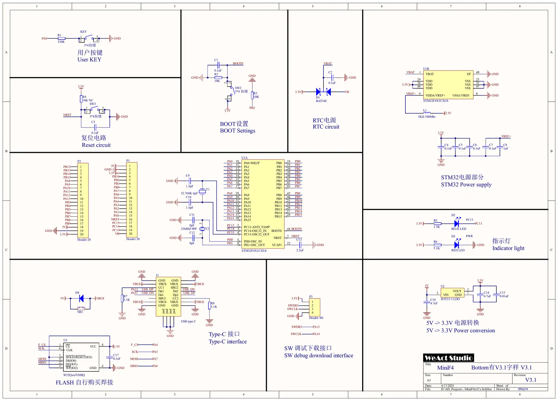
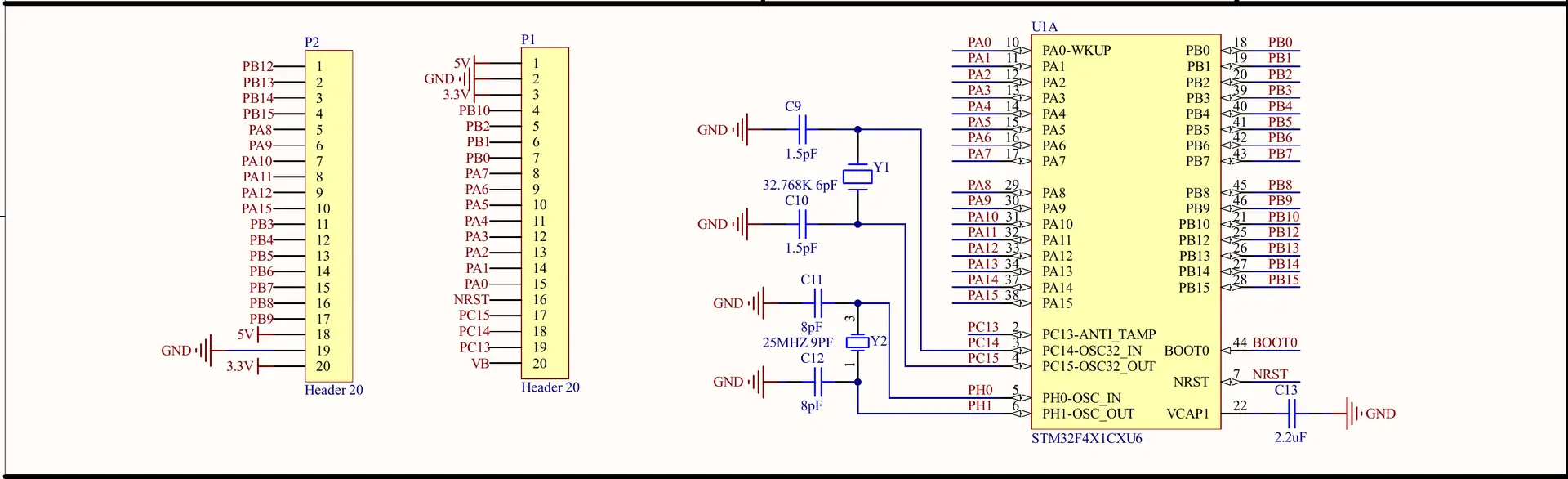
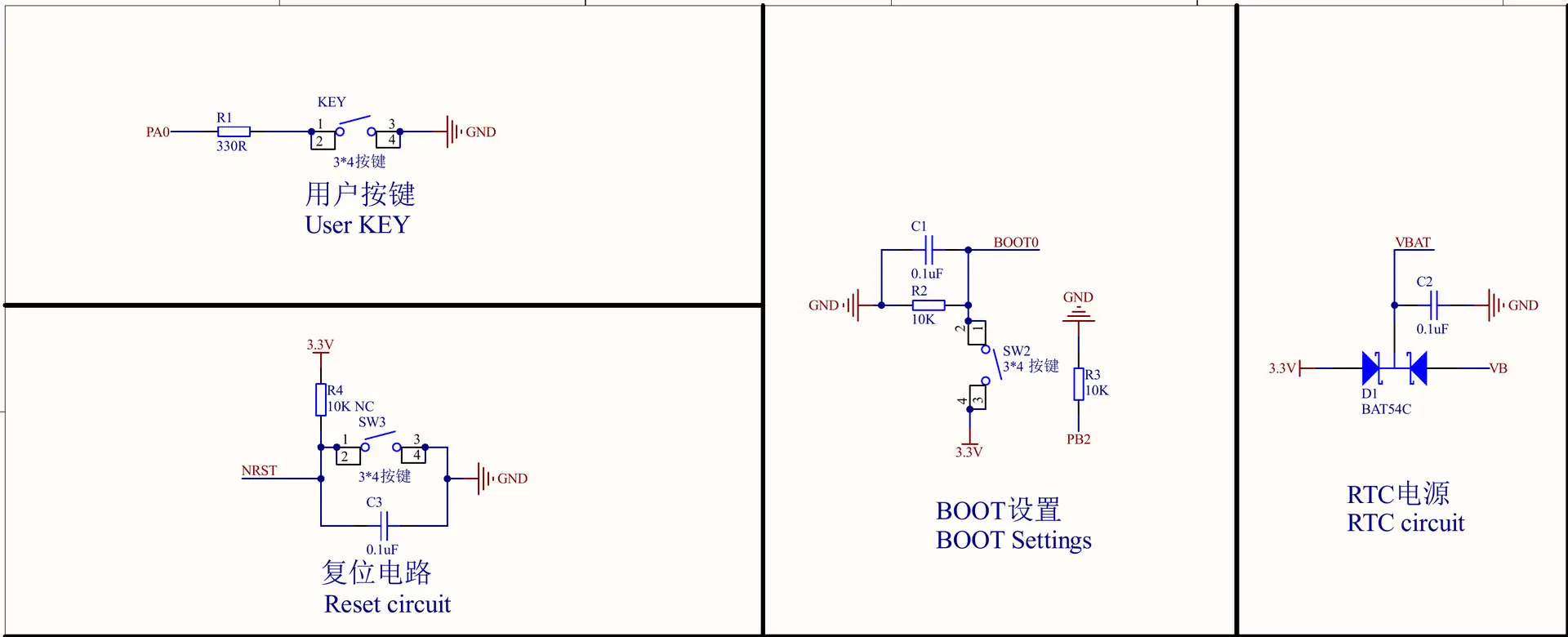
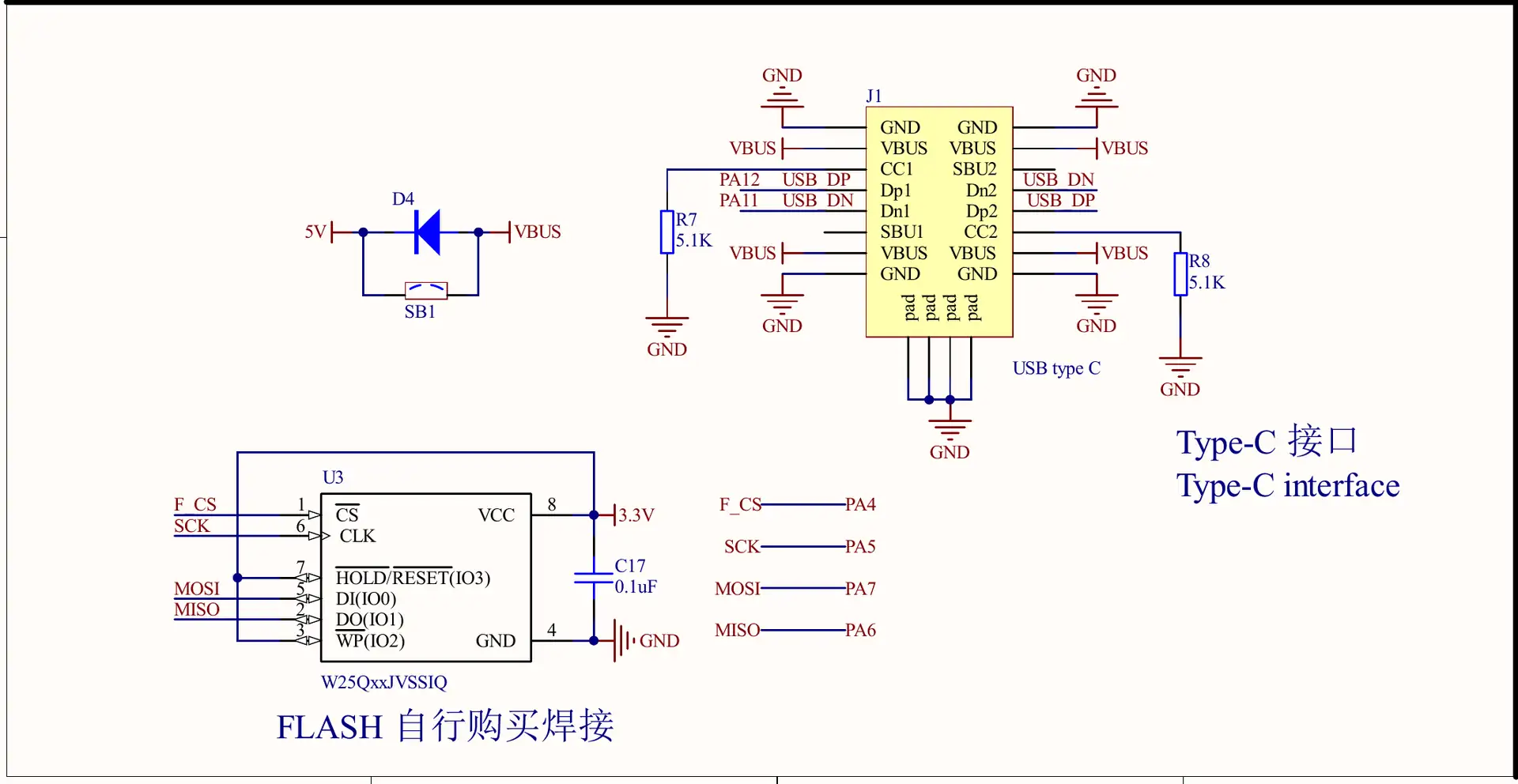
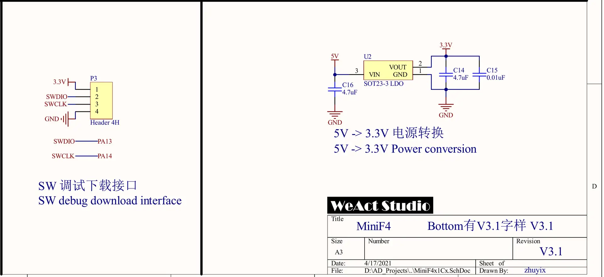
Official source: MiniF4x1Cx V3.1 schematic (PDF) from WeAct’s GitHub repository (Hardware folder; the release notes list what changed in each version). Here’s what to look at:
- Power path: USB-C VBUS goes through the Schottky diode D4 (B5819WS) to the 5V net and the 5V pins. The 5V net feeds the U2 LDO, an ME6231A33M3G on V3.1 (500mA max, 3v–18v input), whose 3.3v output powers the MCU, the LEDs, the 3V3 pins, and the optional flash. VDDA/VREF+ gets the same 3.3v through ferrite L1.
- SB1 (V3.1, bottom side): a solder pad across D4. Bridging it lets the USB-C port output 5v for USB host projects, but it also removes the protection that stops the 5V pins from back-feeding the USB port.
- USB-C: D+ and D− go straight to PA12 and PA11 (USB OTG FS), and CC1/CC2 have 5.1kΩ pull-downs, so any USB-C charger or port supplies 5v. PA9 (VBUS sense) and PA10 (ID) are not connected to the connector.
- Clocks: a 25MHz HSE crystal (Y2) on PH0/PH1, and a 32.768kHz LSE crystal (Y1) on PC14/PC15, which are also on the P1 header.
- Buttons and LEDs: KEY connects PA0 to GND through a 330Ω resistor (no pull-up), BOOT0 has a 10kΩ pull-down and the button pulls it to 3.3v, PB2 (BOOT1) has a 10kΩ pull-down, and the blue LED goes from 3.3v through 1.5kΩ to PC13, so it lights when PC13 is low.
- RTC supply: the BAT54C dual diode (D1) feeds VBAT from whichever is higher, the 3.3v rail or the VB pin, so a coin cell on VB keeps the RTC running when the board is off.
- SPI flash (U3): an empty SOIC-8 footprint on the bottom for a W25Qxx flash, wired to PA4 (CS), PA5 (SCK), PA6 (MISO) and PA7 (MOSI). The schematic labels it “buy and solder yourself”.
Black Pill F401CE Specs
The Black Pill F401CE is WeAct’s MiniF4 core board fitted with the STM32F401CEU6. Here are its specifications, including the board-level parts that chip-only spec lists usually skip.
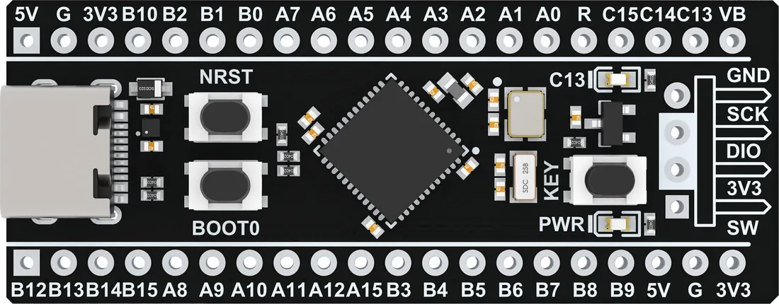
Get an STM32F401 Black Pill: Grab one from Amazon or AliExpress, and check for the STM32F401 chip marking when it arrives.
| Item | Black Pill F401CE |
|---|---|
| MCU | STM32F401CEU6, UFQFPN48 |
| Core | Arm Cortex-M4 with FPU and DSP, up to 84MHz, ART Accelerator |
| Memory | 512KB Flash, 96KB SRAM; optional SPI flash footprint (U3, empty) |
| Logic level | 3.3v (every I/O is 5v tolerant; PB5 must stay ≤ 3.3v per the errata) |
| GPIO pins | 32 on the side headers, plus PA13/PA14 on the SWD header |
| Board supply | USB-C 5v, or 5v into a 5V pin |
| 3.3v regulator | ME6231A33M3G on V3.1 (500mA max, 3v–18v input); “SOT23-3 LDO” on V3.0 |
| Clocks | 25MHz HSE crystal (Y2), 32.768kHz LSE crystal (Y1) |
| USB connector | USB-C (J1), wired to the MCU’s USB 2.0 Full-Speed OTG (PA11/PA12) |
| Debugger | None on board: 4-pin SWD header (P3) for an ST-LINK, or USB DFU / USART bootloader |
| Headers | 2x 20-pin 0.1″ (P1, P2), 15.24mm apart, + 4-pin SWD (P3) |
| User I/O | Blue LED on PC13 (active low), KEY button on PA0, NRST and BOOT0 buttons, red power LED |
| PCB | WeAct MiniF4 V3.1 (V3.0 in the photo), 20.78 × 52.81mm |
| Not Available | DAC, CAN, SDIO (not on this 48-pin package), USB-UART chip |
Black Pill F401CE Specifications Summary
- The Black Pill F401CE runs the STM32F401CEU6 at up to 84MHz with 512KB Flash and 96KB RAM.
- It has 32 GPIOs on the P1/P2 headers, plus PA13/PA14 on the SWD header (34 of the chip’s 36 I/Os; PH0/PH1 drive the crystal).
- Every I/O is 5v tolerant (FT), except in analog mode, and PB5 must never see more than 3.3v (ES0299 errata).
- It has 1x 12-bit ADC (2.4Msps) with all 10 channels on the headers: PA0–PA7, PB0 and PB1.
- 25 header pins can output PWM, from TIM1–TIM5 and TIM9–TIM11.
- It has 3 USARTs. Arduino Serial is USART1 on PA9 (TX) / PA10 (RX); USART6 is only on the USB pins.
- It has 3x I2C. The Arduino Wire pins are PB7 (SDA) and PB6 (SCL).
- It has 3x SPI (two with I²S). The Arduino SPI pins are PA5 (SCK), PA6 (MISO), PA7 (MOSI), with PA4 as SS.
- The USB-C port is the MCU’s own USB 2.0 Full-Speed on PA11/PA12 (DFU, CDC, HID); there’s no USB-UART chip.
- The blue LED is on PC13 (on when LOW), and the KEY button is on PA0 (reads LOW when pressed, needs the internal pull-up).
- The LDO gives 500mA max on V3.1 and also powers the MCU. There’s no DAC and no CAN.
Black Pill F401CE Peripherals: MCU vs On the Headers
The STM32F401CE in its 48-pin package loses some of the family’s pins. This table tells you what the chip has and what you can actually reach on the board.
| Peripheral | STM32F401CE (UFQFPN48) | On the Black Pill headers |
|---|---|---|
| GPIO | 36 I/Os | 32 on P1/P2 + PA13/PA14 on SWD; PH0/PH1 are the 25MHz crystal |
| ADC | 1x 12-bit, 2.4Msps, 10 external channels | all 10 (PA0–PA7, PB0, PB1) |
| Timers | TIM1 (advanced), TIM2/TIM5 (32-bit), TIM3, TIM4, TIM9–TIM11 | 25 PWM pins |
| USART | USART1, USART2, USART6 | all 3; USART6 only on PA11/PA12 (the USB pins) |
| SPI / I²S | SPI1, SPI2, SPI3; I²S2, I²S3 | all 3 (SPI4 is not bonded out on 48 pins) |
| I²C | I2C1, I2C2, I2C3 | all 3 |
| USB | USB 2.0 OTG Full-Speed | on the USB-C connector (VBUS sense and ID not wired) |
| SDIO | not on the 48-pin package | – |
| DAC, CAN | none on the STM32F401 | – |
Black Pill F401CE Quick Pin Selection Guide
Not sure which pin to use? Here are the Black Pill F401CE pins I’d pick first for each job, and why.
| Use Case | Recommended Pins | Why |
|---|---|---|
| Serial to the PC | USB-C (USB CDC) | No USB-UART chip on the board; enable USB CDC in your firmware |
| Serial to a module (GPS, Bluetooth…) | USART2: PA2 (TX), PA3 (RX) | Leaves USART1 (PA9/PA10) free for the bootloader and Serial |
| I2C sensors and displays | PB6 (SCL), PB7 (SDA) | The Arduino Wire pins; add 4.7kΩ pull-ups |
| SPI devices | PA5 (SCK), PA6 (MISO), PA7 (MOSI), PA4 (CS) | The Arduino SPI pins; or SPI2 on PB13–PB15 + PB12 |
| PWM (motors, LEDs, servos) | PB6–PB9 (TIM4), PA8–PA10 (TIM1), PA1–PA3 (TIM2) | Four channels on one timer share a frequency |
| Analog inputs | PA1, PA2, PA3, PB0, PB1 | Free ADC pins with no button or flash on them |
| USB device | USB-C (PA11/PA12) | Already wired; CDC, HID, MSC or DFU |
| External interrupt | Any GPIO (one pin per EXTI line) | PA0 (KEY) is already a button |
| On-board LED / button | PC13 (LED), PA0 (KEY) | LED_BUILTIN and USER_BTN in Arduino |
| Safest general GPIO | PB12–PB15, PB10, PB0, PB1, PA1–PA3 | No board load and no debug or boot role |
Black Pill F401CE Pins to Use With Caution
| Pin | Reason | What to Do |
|---|---|---|
| PA11, PA12 | USB D− / D+, wired to the USB-C connector | Keep them for USB; using them as GPIO or USART6 breaks USB |
| PA13, PA14 | SWD pins (SWDIO, SWCLK) | Don’t reuse them, or you lose debugging |
| PB3, PB4, PA15 | JTAG pins (SWO, NJTRST, JTDI) after reset | Set debug to Serial Wire to free them |
| PB5 | Must never exceed VDD (ES0299: I/O leakage) | Never connect 5v signals here, even though it’s FT |
| PC13, PC14, PC15 | Backup-domain pins: 3mA sink max, 2MHz max, never a current source | PC13 has the LED, PC14/PC15 the 32.768kHz crystal; use them for slow inputs |
| PA0 | KEY button to GND (330Ω); must not exceed VDD in Standby (errata) | Use the internal pull-up; don’t drive it hard while the button is pressed |
| PA4–PA7 | Go to the optional SPI flash footprint | Free by default; if you fit a flash chip, they’re its SPI1 bus |
| PA9, PA10 | USART1, the system bootloader UART | Keep PA10 quiet (or low) while entering DFU |
| PB2 | BOOT1, 10kΩ pull-down | Keep it LOW at reset if you use the system bootloader |
Black Pill F401CE Pins Functions
The 40 header pins of the Black Pill F401CE (plus the 4-pin SWD header) are divided into the following groups based on the hardware functionality they’re used for. Most pins have several alternate functions, so one pin can belong to more than one group.
- Power Pins: 5V, 3V3, VB, GND
- 32x Digital GPIO Pins (+ PA13/PA14 on SWD)
- 16x External Interrupt Lines (any GPIO)
- 10x ADC Analog Input Pins
- 25x PWM Pins
- 3x UART Ports
- 3x I2C Buses
- 3x SPI Ports
- 1x USB OTG Port (USB-C)
- Debug (SWD) & Boot Pins
We’ll discuss each pin group in the following sections one by one in more detail.
Black Pill F401CE Power Pins
The Black Pill F401CE is powered from the USB-C connector (5v) or from 5v on a 5V pin. An on-board LDO makes the 3.3v rail for the MCU and the 3V3 pins, and the VB pin can take a coin cell for the RTC. The power pins are highlighted in red in the pinout diagram.
| Pin | Header Pins | Range | Notes |
|---|---|---|---|
| 5V | P2-18, P1-1 | 5v in / out | USB-C 5v minus the D4 diode drop when USB is plugged in; feed 5v here when it isn’t |
| 3V3 | P2-20, P1-3, P3-1 | 3.3v out | LDO output (ME6231A33M3G, 500mA max on V3.1), shared with the MCU and LEDs |
| VB | P1-20 | coin cell | VBAT for the RTC and backup registers, through the BAT54C diode |
| GND | P2-19, P1-2, P3-4 | 0v | All grounds are common |
Diode D4 blocks a 5v supply on the 5V pins from flowing back into your PC’s USB port, so it’s safe to have both connected. The 3.3v LDO also powers the MCU and the LEDs, so plan your external 3.3v loads with some margin below the 500mA limit, and power motors or LED strips from their own supply.
Note: Do not feed 5v into a 3V3 pin. And if you bridge the SB1 pad on the back (V3.1), D4 is shorted, so a supply on the 5V pins goes straight into the USB-C port: never plug the board into a PC with SB1 bridged and an external 5v supply connected.
Black Pill F401CE GPIO Pins
The Black Pill F401CE has 32 GPIO pins on its two side headers, plus PA13/PA14 on the SWD header. They work at 3.3v, and all of them are 5v tolerant as digital inputs, with one exception from the errata: PB5.
Each GPIO can be an input (floating, pull-up or pull-down), a push-pull or open-drain output, an analog pin or an alternate function. The internal pull-up/pull-down resistors are about 40kΩ. Here are the electrical limits from the DS10086 datasheet:
- Absolute max current per pin: ±25mA. Keep it under ±8mA for guaranteed logic levels.
- Total current sunk by all pins: 120mA, and 160mA total into the VDD pins.
- PC13, PC14 and PC15: 3mA sink max, 2MHz max, never as a current source.
- 5v tolerance (FT) only applies while the pin isn’t in analog mode, and not for PC14/PC15 while the LSE crystal runs.
Note: The ES0299 errata says PB5 must never see a voltage above VDD, because of an I/O leakage that can shorten the chip’s life, even though the datasheet lists it as FT. On the Black Pill F401CE, treat PB5 as a 3.3v-only pin, and use a level shifter if a 5v signal must go there. PA0 has a similar limit, but only in Standby mode.
Learn more in our STM32 GPIO Tutorial series.
Also Read
Black Pill F401CE Interrupt Pins
Every GPIO pin on the Black Pill F401CE can be an external interrupt source. The STM32F401CE has 16 EXTI lines for the pins, one per pin number, so PA0 and PB0 share EXTI0 and only one of them can use it at a time.
| EXTI Line | Pins That Can Use It | Interrupt Vector |
|---|---|---|
| EXTI0 – EXTI4 | Px0 – Px4 (one port each) | EXTI0_IRQn … EXTI4_IRQn (one each) |
| EXTI5 – EXTI9 | Px5 – Px9 | EXTI9_5_IRQn (shared) |
| EXTI10 – EXTI15 | Px10 – Px15 (PC13 on EXTI13) | EXTI15_10_IRQn (shared) |
The KEY button on PA0 is the easiest pin to try an interrupt with: enable the internal pull-up, and it reads LOW when pressed, so set a falling-edge trigger. In Arduino, attachInterrupt(digitalPinToInterrupt(PA0), isr, FALLING) after pinMode(PA0, INPUT_PULLUP).
Learn more in our STM32 External Interrupt Tutorial series.
Also Read
Black Pill F401CE ADC Pins
The Black Pill F401CE has 1x 12-bit ADC with 10 external channels, and all 10 are on the headers: PA0–PA7, PB0 and PB1. The ADC reference is the 3.3v rail (through ferrite L1), so the input range is 0v to 3.3v.
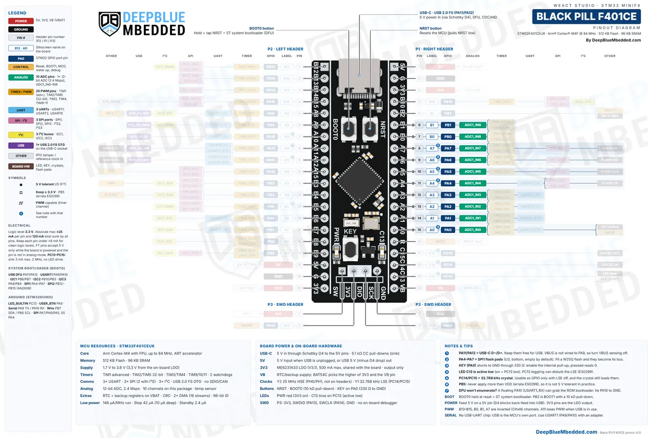
| GPIO | ADC Channel | Header Pin | Note |
|---|---|---|---|
| PA0 | ADC1_IN0 | P1-15 | KEY button to GND |
| PA1 | ADC1_IN1 | P1-14 | |
| PA2 | ADC1_IN2 | P1-13 | USART2_TX |
| PA3 | ADC1_IN3 | P1-12 | USART2_RX |
| PA4 | ADC1_IN4 | P1-11 | Flash CS footprint |
| PA5 | ADC1_IN5 | P1-10 | Flash CLK footprint |
| PA6 | ADC1_IN6 | P1-9 | Flash DO footprint |
| PA7 | ADC1_IN7 | P1-8 | Flash DI footprint |
| PB0 | ADC1_IN8 | P1-7 | |
| PB1 | ADC1_IN9 | P1-6 |
The ADC converts at up to 2.4Msps and has an internal temperature sensor and VREFINT channel too. All the ADC pins sit together on the P1 header, which makes analog wiring easy.
Note: A pin in analog mode is never 5v tolerant, so keep every ADC input between 0v and 3.3v. Use a voltage divider to measure higher voltages.
There are so many sensors that we can read with the ADC pins, which include: potentiometers, LDRs, analog temperature sensors (LM35, NTC thermistors), current sensors (ACS712), joysticks, soil moisture sensors, and much more.
Learn more in our STM32 ADC Tutorial series.
Also Read
Black Pill F401CE PWM Pins
The Black Pill F401CE has 25 PWM pins on its headers, driven by TIM1 (advanced), TIM2 and TIM5 (32-bit), TIM3, TIM4, and TIM9–TIM11. The PWM pins are highlighted in orange in the pinout diagram.
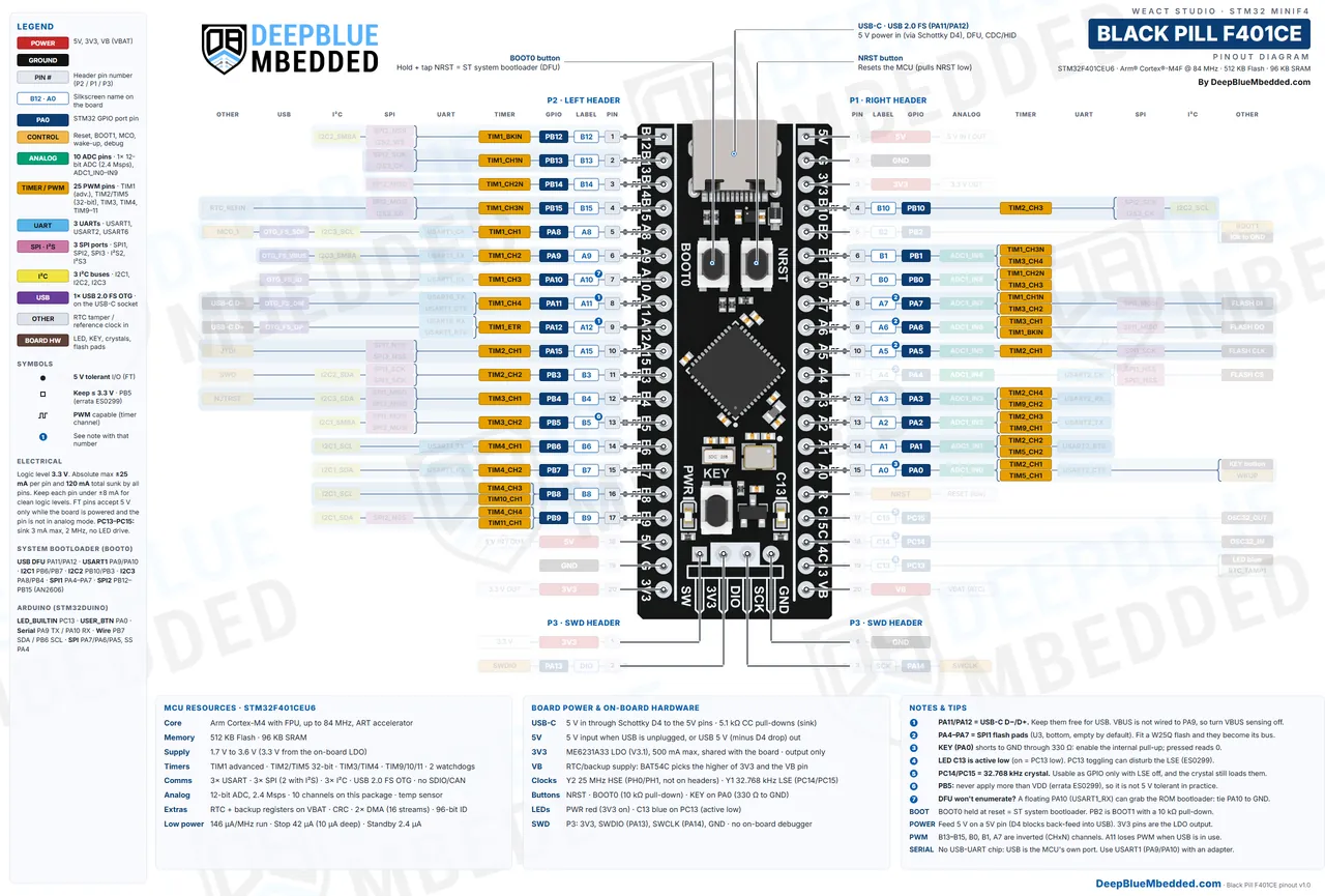
| Timer | PWM Pins (Channel) |
|---|---|
| TIM1 (advanced) | PA8 (CH1), PA9 (CH2), PA10 (CH3), PA11 (CH4); PB13/PA7 (CH1N), PB14/PB0 (CH2N), PB15/PB1 (CH3N) |
| TIM2 (32-bit) | PA0/PA5/PA15 (CH1), PA1/PB3 (CH2), PA2/PB10 (CH3), PA3 (CH4) |
| TIM3 | PA6/PB4 (CH1), PA7/PB5 (CH2), PB0 (CH3), PB1 (CH4) |
| TIM4 | PB6 (CH1), PB7 (CH2), PB8 (CH3), PB9 (CH4) |
| TIM5 (32-bit) | PA0 (CH1), PA1 (CH2), PA2 (CH3), PA3 (CH4) |
| TIM9 | PA2 (CH1), PA3 (CH2) |
| TIM10 / TIM11 | PB8 (TIM10_CH1), PB9 (TIM11_CH1) |
Pins on the same timer share its frequency, and the CHxN pins (PB13–PB15, PB0, PB1, PA7 on TIM1) are the inverted complementary outputs, made for motor drivers with dead-time. PA11 (TIM1_CH4) is a USB pin, so it’s only a PWM pin if you don’t use USB.
There are so many things that we can control with PWM, which include: LED dimming, DC motor speed (with a driver), servo motors, buzzers, ESCs for brushless motors, and much more.
Calculate your timer settings with this STM32 PWM Calculator.
Learn more in our STM32 PWM Tutorial series.

Also Read
Black Pill F401CE UART Pins
The Black Pill F401CE has 3 USARTs: USART1, USART2 and USART6. USART1 on PA9 (TX) / PA10 (RX) is the default Arduino Serial and the system bootloader’s UART. There’s no USB-UART chip, so to talk to a PC you either use USB CDC on the USB-C port or a USB-serial adapter on these pins.
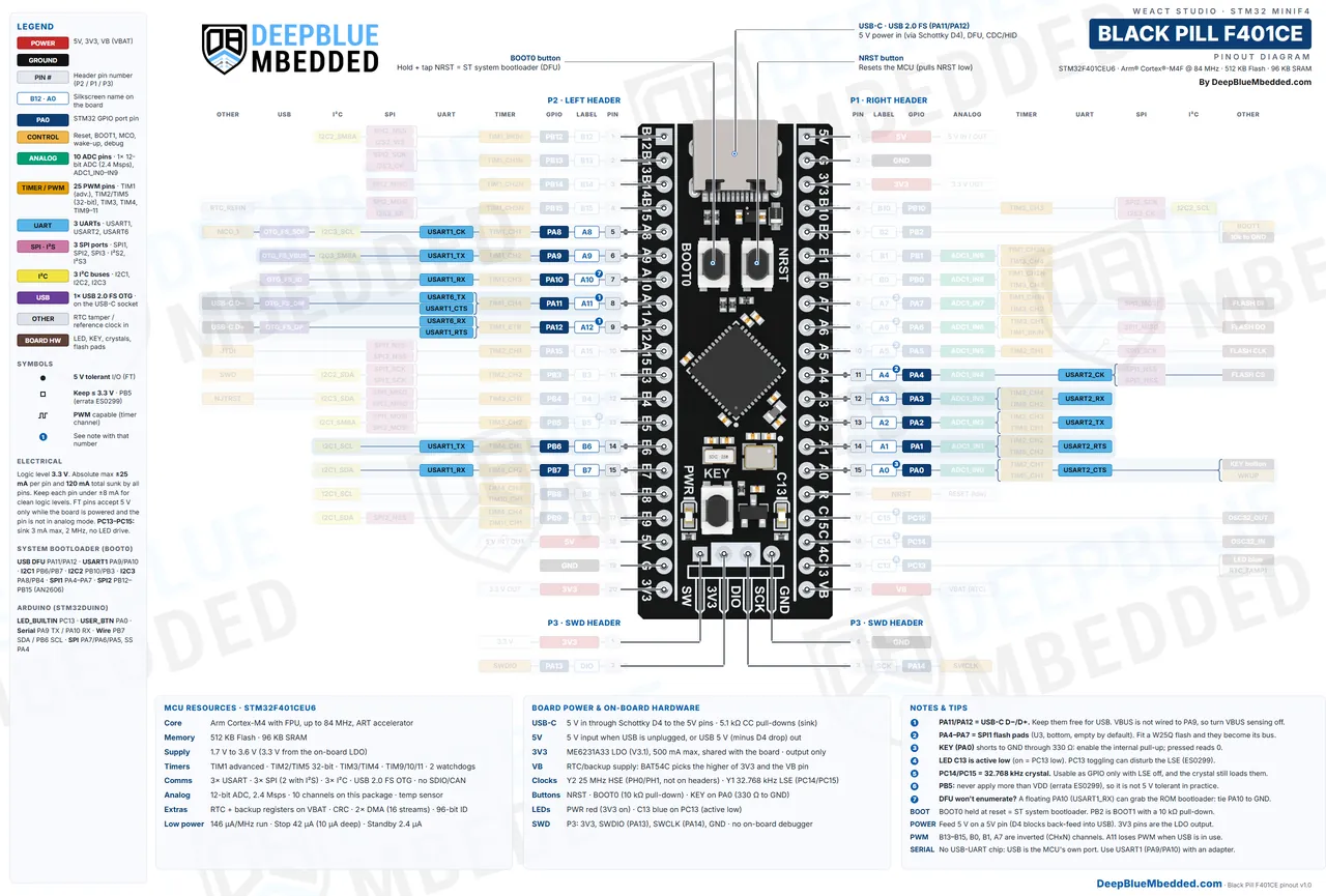
Black Pill F401CE Default Serial (USART1): PA9 (TX) and PA10 (RX).
| UART | TX Pins | RX Pins | Note |
|---|---|---|---|
| USART1 | PA9 (P2-6), PB6 (P2-14) | PA10 (P2-7), PB7 (P2-15) | Arduino Serial; system bootloader UART |
| USART2 | PA2 (P1-13) | PA3 (P1-12) | Best free UART for a module; RTS/CTS on PA1/PA0 |
| USART6 | PA11 (P2-8) | PA12 (P2-9) | Only on the USB pins, so not usable with USB |
Note: A 3.3v USB-serial adapter connects TX to RX and RX to TX: adapter TX → PA10, adapter RX → PA9, plus GND. The pins are 5v tolerant, but a 3.3v adapter is the safe choice.
There are so many modules that we can interface with the UART pins, which include: GPS modules, Bluetooth modules (HC-05), ESP8266/ESP32 Wi-Fi modules, GSM modules, RS485 transceivers, fingerprint sensors, and much more.
Learn more in our STM32 UART Tutorial series.
Also Read
Black Pill F401CE I2C Pins
The Black Pill F401CE has 3x I2C buses. The default Arduino Wire pins are PB6 (SCL) and PB7 (SDA) on I2C1, and I2C1 can also use PB8 (SCL) / PB9 (SDA), which is what Zephyr uses.
Black Pill F401CE Default I2C1 Pins: PB7 (SDA) and PB6 (SCL).
| I2C Bus | SCL Pins | SDA Pins | Note |
|---|---|---|---|
| I2C1 | PB6 (P2-14), PB8 (P2-16) | PB7 (P2-15), PB9 (P2-17) | Arduino Wire on PB6/PB7 |
| I2C2 | PB10 (P1-4) | PB3 (P2-11) | PB3 is SWO after reset: set debug to Serial Wire |
| I2C3 | PA8 (P2-5) | PB4 (P2-12) | PB4 is NJTRST after reset: set debug to Serial Wire |
Note: There are no I2C pull-up resistors on the board, so add 4.7kΩ pull-ups to 3.3v unless your module already has them. And note that I2C2 has its SCL on the P1 header (PB10) and its SDA on the P2 header (PB3).
There are so many modules and sensors that we can interface with the I2C bus, which include: OLED displays (SSD1306), I2C LCDs, RTC modules (DS3231), IMUs (MPU6050), BME280 sensors, EEPROMs, and much more.
Learn more in our STM32 I2C Tutorial series.
Also Read
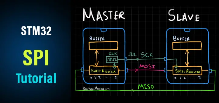
Black Pill F401CE SPI Pins
The Black Pill F401CE has 3x SPI ports (SPI1, SPI2, SPI3), and SPI2/SPI3 can also run as I²S for audio. The default Arduino SPI pins are PA5 (SCK), PA6 (MISO) and PA7 (MOSI) on SPI1, with PA4 as SS.
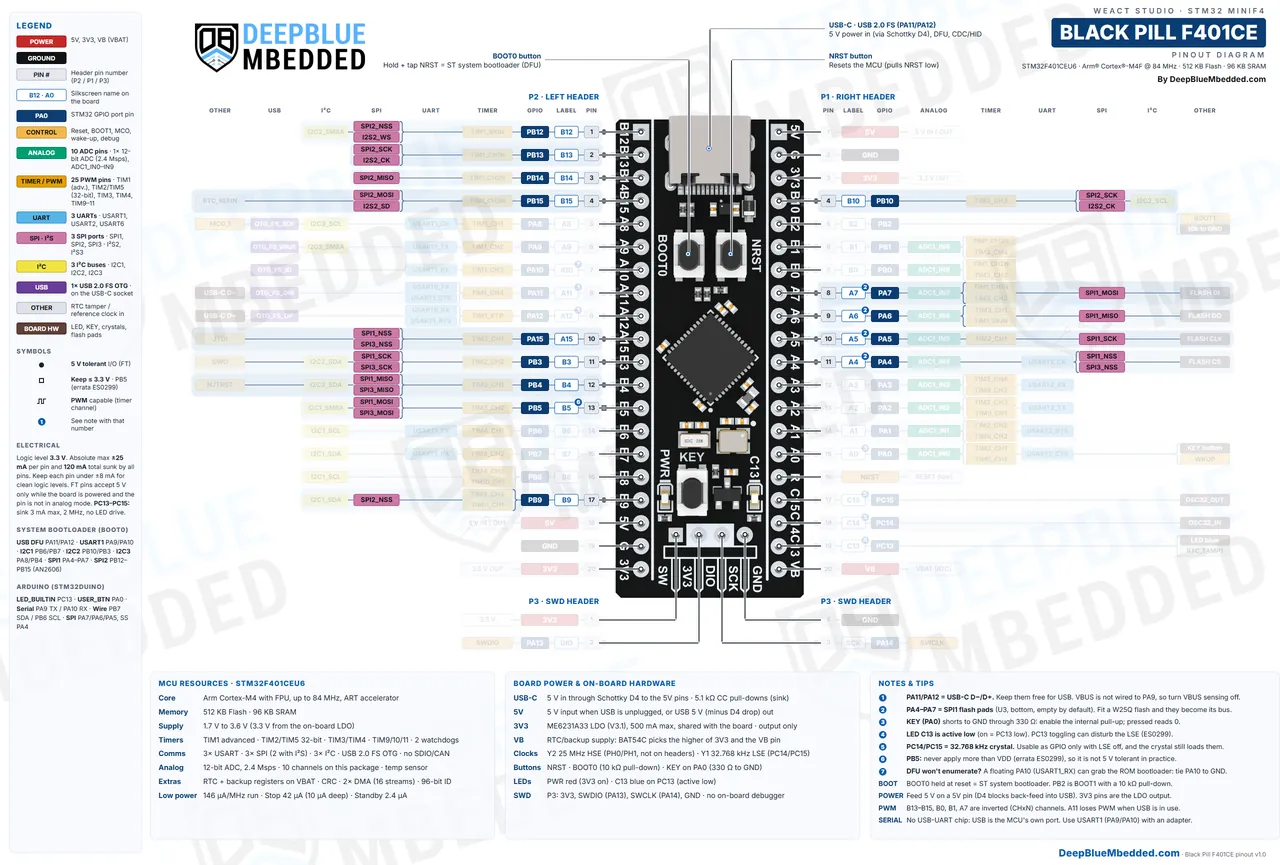
Black Pill F401CE Default SPI1 Pins: PA5 (SCK), PA6 (MISO), PA7 (MOSI), and PA4 (SS).
| SPI Port | SCK | MISO | MOSI | NSS |
|---|---|---|---|---|
| SPI1 | PA5, PB3 | PA6, PB4 | PA7, PB5 | PA4, PA15 |
| SPI2 / I²S2 | PB13, PB10 | PB14 | PB15 | PB12, PB9 |
| SPI3 / I²S3 | PB3 | PB4 | PB5 | PA15, PA4 |
Note: PA4–PA7 also go to the empty SPI flash footprint on the back. If you solder a W25Qxx flash chip there, it sits on SPI1 with PA4 as its chip select, so put your other SPI devices on SPI2 (PB12–PB15).
There are so many modules that we can interface with the SPI bus, which include: TFT displays (ILI9341, ST7735), SD card modules, nRF24L01 radios, MAX7219 LED drivers, W5500 Ethernet modules, and much more.
Learn more in our STM32 SPI Tutorial series.
Also Read
Black Pill F401CE USB Pins
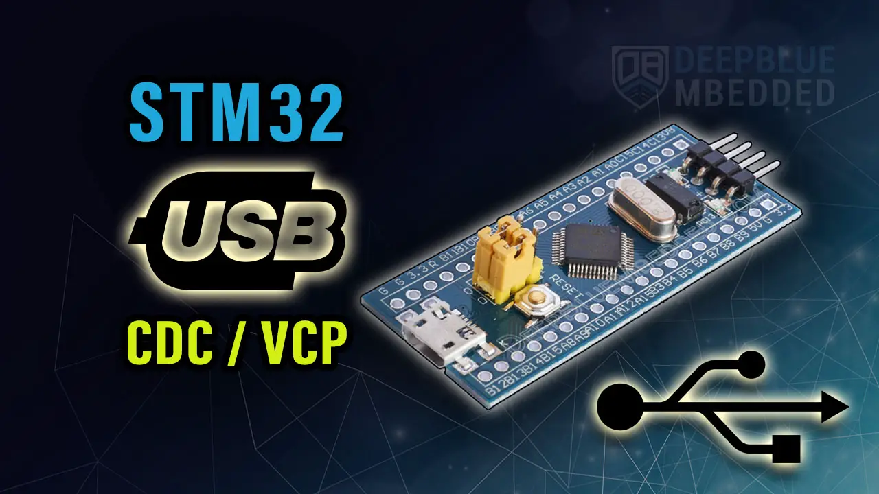
The Black Pill F401CE’s USB-C connector is wired straight to the STM32F401CE’s USB 2.0 Full-Speed OTG controller on PA11 (D−) and PA12 (D+). That’s how the board gets USB DFU flashing, a virtual COM port (CDC), HID or mass storage, with no extra chip.
| Signal | GPIO | On This Board |
|---|---|---|
| D− (DM) | PA11 (P2-8) | Wired to the USB-C connector |
| D+ (DP) | PA12 (P2-9) | Wired to the USB-C connector |
| VBUS sense | PA9 (P2-6) | Not connected: turn VBUS sensing off |
| ID | PA10 (P2-7) | Not connected |
| SOF | PA8 (P2-5) | Optional start-of-frame output |
Note: PA9 is not connected to USB VBUS on this board. In CubeMX, leave “VBUS sensing” disabled for the USB device, otherwise the USB stack waits for a VBUS signal that never arrives and the PC never sees the board.
USB needs an exact 48MHz clock. From the 25MHz crystal, set PLLM = 25, PLLN = 336, PLLP = 4 and PLLQ = 7 to get 84MHz for the core and 48MHz for USB.
Learn more in our STM32 USB CDC Tutorial.
Also Read
Black Pill F401CE Debug (SWD) & Boot Pins
The Black Pill F401CE is programmed and debugged over SWD on the 4-pin header P3: 3V3, SWDIO (PA13), SWCLK (PA14) and GND. The boot mode is set by the BOOT0 button and PB2 (BOOT1), which has a 10kΩ pull-down.
| Pin | Header Pin | Function After Reset |
|---|---|---|
| 3V3 | P3-1 (square pad) | 3.3v (for the debugger’s target voltage sense) |
| PA13 | P3-2 (DIO) | SWDIO |
| PA14 | P3-3 (SCK) | SWCLK |
| GND | P3-4 | Ground |
| NRST | P1-16 (R) | Reset (NRST button) |
| PB3 | P2-11 | SWO (JTDO) |
| PA15 | P2-10 | JTDI |
| PB4 | P2-12 | NJTRST |
| PB2 (BOOT1) | P1-5 | Pulled LOW by 10kΩ |
| BOOT0 | BOOT1 (PB2) | Boots From |
|---|---|---|
| 0 (button released) | any | Main Flash (normal) |
| 1 (button held) | 0 | System memory (ST bootloader: USB DFU, USART1, I2C, SPI) |
| 1 | 1 | Embedded SRAM |
To start the ST system bootloader, hold BOOT0, tap NRST, and release BOOT0 about half a second later (or hold BOOT0 while you plug in the USB cable). The board then shows up as “STM32 BOOTLOADER” (DFU), and STM32CubeProgrammer can flash it over USB. AN2606 also lists USART1 (PA9/PA10), I2C1–I2C3 and SPI1/SPI2 as bootloader interfaces on this chip.
Note: The P3 header has no reset pin. If your firmware reconfigures PA13/PA14 and the ST-LINK can’t connect anymore, use “Connect under reset” with a wire from NRST (P1-16) to the ST-LINK, or hold the BOOT0 button while you reset so the MCU starts the bootloader instead of your code.
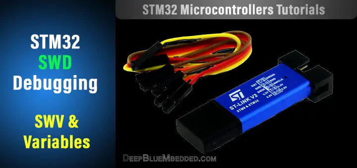
Learn more in our STM32 SWD Debugging Tutorial.
Also Read
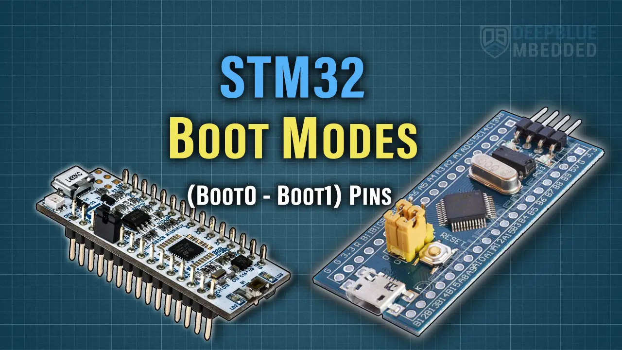
Learn more in our STM32 Boot Modes Tutorial.
Also Read
Black Pill F401CE On-Board Features
Besides the headers, the Black Pill F401CE has 2 LEDs, 3 buttons, 2 crystals, and a couple of footprints and pads on the back. Here’s what each one does.
| Part | Pin / Connection | What It Does |
|---|---|---|
| PWR LED (red, D3) | 3.3v → 5.1kΩ → GND | On whenever the 3.3v rail is up |
| C13 LED (blue, D2) | 3.3v → 1.5kΩ → PC13 | On when PC13 is LOW (active low) |
| KEY button | PA0 → 330Ω → GND | Reads LOW when pressed; needs the internal pull-up |
| BOOT0 button | BOOT0 → 3.3v (10kΩ pull-down) | Held during reset: start the system bootloader |
| NRST button | NRST → GND | Resets the MCU |
| Y2 crystal | PH0/PH1 | 25MHz HSE for the PLL and USB |
| Y1 crystal | PC14/PC15 | 32.768kHz LSE for the RTC |
| U3 footprint (bottom) | PA4–PA7 | Empty SOIC-8 for a W25Qxx SPI flash |
| SB1 pad (bottom, V3.1) | Across diode D4 | Bridge it to let the USB-C port output 5v (USB host) |
Getting Started With Black Pill F401CE
You can program the Black Pill F401CE with any of the common STM32 toolchains. You don’t even need a debugger to start: the ST bootloader’s USB DFU mode flashes it over the USB-C cable. An ST-LINK on the SWD header adds real debugging.
- STM32CubeIDE: start a new project for the STM32F401CEUx, set RCC → HSE to “Crystal/Ceramic Resonator” (25MHz), set SYS → Debug to “Serial Wire”, and configure PC13 as an output for the LED. Flash it with an ST-LINK, or with STM32CubeProgrammer over DFU.
- Arduino IDE (STM32duino): install “STM32 MCU based boards”, then choose Board: “Generic STM32F4 series” and Board part number: “BlackPill F401CE”. Pick “STM32CubeProgrammer (DFU)” or “(SWD)” as the upload method.
- PlatformIO: board ID blackpill_f401ce, with the STM32Cube or Arduino framework.
- Zephyr RTOS: board name blackpill_f401ce.
- MicroPython: WeAct publishes a MicroPython build for the F401CE in its GitHub repository (SDK folder).
| Arduino Name | Pin | Default |
|---|---|---|
Serial | PA9 (TX) / PA10 (RX) | USART1 (enable “USB CDC” in the Tools menu to get Serial over USB-C) |
Wire | PB7 (SDA), PB6 (SCL) | I2C1 |
SPI | PA5 / PA6 / PA7, SS = PA4 | SPI1 |
LED_BUILTIN | PC13 | Blue LED, active low |
USER_BTN | PA0 | KEY button |
Here’s a first test that blinks the blue LED and prints the KEY button state at 115200 baud:
|
1 2 3 4 5 6 7 8 9 10 11 |
void setup() { pinMode(LED_BUILTIN, OUTPUT); // blue LED on PC13 (on when LOW) pinMode(USER_BTN, INPUT_PULLUP); // KEY on PA0, LOW when pressed Serial.begin(115200); // USART1 on PA9/PA10, or USB CDC } void loop() { digitalWrite(LED_BUILTIN, !digitalRead(LED_BUILTIN)); Serial.println(digitalRead(USER_BTN) ? "KEY released" : "KEY pressed"); delay(500); } |
With STM32CubeIDE and HAL, the same blink is HAL_GPIO_TogglePin(GPIOC, GPIO_PIN_13); in the main loop. Follow the STM32 LED Blink Code Example for the full walk-through, and set up the 84MHz clock with the STM32 RCC Clock Configuration Guide (PLL from the 25MHz HSE, 2 Flash wait states).
Black Pill STM32F401CE Common Problems & Fixes
Why isn’t my Black Pill recognized in DFU mode? Two known causes. A floating PA10 (USART1_RX) can pick up noise, and the ROM bootloader then picks USART1 instead of USB, so keep PA9/PA10 unconnected or tie PA10 to GND while you enter DFU (stm32duino forum). And the bootloader has to detect the 25MHz crystal against the internal oscillator, which AN2606 says is harder at high HSE values; WeAct’s own tip is to warm the chip a little, or just retry. If DFU still fails, flash over SWD or USART1.
Why does the LED turn on when I write LOW? The blue LED is wired from 3.3v to PC13, so it’s active low: digitalWrite(LED_BUILTIN, LOW) turns it on.
Why does the KEY button always read the same? The KEY button connects PA0 to GND, and there’s no pull-up resistor on the board. Use INPUT_PULLUP (or the CubeMX pull-up), and it reads LOW when pressed.
Why doesn’t Serial show anything on my PC? There’s no USB-UART chip. Serial is USART1 on PA9/PA10, so either connect a USB-serial adapter there, or enable USB CDC in the Arduino Tools menu (or a CDC device in CubeMX) to get a COM port over USB-C.
Why doesn’t my USB device show up on the PC? Check that VBUS sensing is off (PA9 isn’t connected to VBUS) and that the PLL gives exactly 48MHz to USB (PLLQ = 7 with a 25MHz crystal and PLLN = 336).
Why don’t PB3, PB4 and PA15 toggle? They’re JTAG pins after reset. In CubeMX, set SYS → Debug to “Serial Wire”, which frees them.
Why did the RTC drift while the LED was blinking? The ES0299 errata says toggling PC13 can disturb the 32.768kHz LSE crystal on this package. If you need an accurate RTC, don’t blink the C13 LED fast, or use another pin for activity.
STM32 Black Pill: F401CE vs F401CC vs F411CE
WeAct built three Black Pill versions on the same MiniF4 PCB, so the headers, power, LEDs and buttons are identical and the Black Pill F401CE pinout applies to all of them. Only the MCU changes:
| Feature | Black Pill F401CC | Black Pill F401CE | Black Pill F411CE |
|---|---|---|---|
| MCU | STM32F401CCU6 | STM32F401CEU6 | STM32F411CEU6 |
| Clock | 84MHz | 84MHz | 100MHz |
| Flash / RAM | 256KB / 64KB | 512KB / 96KB | 512KB / 128KB |
| SPI / I²S | 3 / 2 | 3 / 2 | 5 / 5 |
| UART / I2C / ADC | 3 / 3 / 10 ch | 3 / 3 / 10 ch | 3 / 3 / 10 ch |
| WeAct status | Discontinued | Discontinued | On sale |
Pick the Black Pill F401CE if you already have one, or when you need twice the Flash of the F401CC. For a new project, the F411CE is the better buy: it’s still in production, faster, and has more RAM, and everything on this page applies to it too. See the STM32F411 Black Pill Pinout guide for that board, or the STM32 Blue Pill Pinout guide if you’re comparing it with the older STM32F103 board.
Black Pill STM32F401CE Pin Details
Here is every Black Pill F401CE header pin in physical order, with its main functions, all its alternate functions, its 5v tolerance, and a short description. Pin 1 of each header has the square pad; with the USB-C connector at the top, P2 is the left header and P1 the right one.
Black Pill F401CE P2 Left Header Pins
| Pin | Label | GPIO | Main Functions | All Alternate Functions | 5v Tolerant | Description |
|---|---|---|---|---|---|---|
| P2-1 | B12 | PB12 | TIM1_BKIN, SPI2_NSS, I2S2_WS, I2C2_SMBA | I2C2_SMBA, I2S2_WS, SPI2_NSS, TIM1_BKIN | Yes | SPI2_NSS / I2S2_WS and TIM1_BKIN; a free general-purpose pin with no board load. |
| P2-2 | B13 | PB13 | TIM1_CH1N, SPI2_SCK, I2S2_CK | I2S2_CK, SPI2_SCK, TIM1_CH1N | Yes | SPI2_SCK and TIM1_CH1N (inverted PWM output); free by default. |
| P2-3 | B14 | PB14 | TIM1_CH2N, SPI2_MISO | I2S2_ext_SD, SPI2_MISO, TIM1_CH2N | Yes | SPI2_MISO and TIM1_CH2N (inverted PWM output); free by default. |
| P2-4 | B15 | PB15 | TIM1_CH3N, SPI2_MOSI, I2S2_SD, RTC_REFIN | ADC1_EXTI15, I2S2_SD, RTC_REFIN, SPI2_MOSI, TIM1_CH3N | Yes | SPI2_MOSI, TIM1_CH3N (inverted PWM output) and RTC_REFIN; free by default. |
| P2-5 | A8 | PA8 | TIM1_CH1, USART1_CK, I2C3_SCL, OTG_FS_SOF, MCO_1 | I2C3_SCL, RCC_MCO_1, TIM1_CH1, USART1_CK, USB_OTG_FS_SOF | Yes | TIM1_CH1 PWM, I2C3_SCL, the MCO1 clock output and USART1_CK. |
| P2-6 | A9 | PA9 | TIM1_CH2, USART1_TX, I2C3_SMBA, OTG_FS_VBUS | I2C3_SMBA, TIM1_CH2, USART1_TX, USB_OTG_FS_VBUS | Yes | USART1_TX (the Arduino Serial TX and the bootloader UART) and TIM1_CH2 PWM; not wired to USB VBUS on this board. |
| P2-7 | A10 | PA10 | TIM1_CH3, USART1_RX, OTG_FS_ID | TIM1_CH3, USART1_RX, USB_OTG_FS_ID | Yes | USART1_RX (the Arduino Serial RX and the bootloader UART) and TIM1_CH3 PWM; keep it quiet or tied low while entering DFU. |
| P2-8 | A11 | PA11 | TIM1_CH4, USART6_TX, USART1_CTS, OTG_FS_DM, USB-C D− | ADC1_EXTI11, TIM1_CH4, USART1_CTS, USART6_TX, USB_OTG_FS_DM | Yes | USB D− on the USB-C connector; also USART6_TX and TIM1_CH4, but only if you give up USB. |
| P2-9 | A12 | PA12 | TIM1_ETR, USART6_RX, USART1_RTS, OTG_FS_DP, USB-C D+ | TIM1_ETR, USART1_RTS, USART6_RX, USB_OTG_FS_DP | Yes | USB D+ on the USB-C connector; also USART6_RX and TIM1_ETR, but only if you give up USB. |
| P2-10 | A15 | PA15 | TIM2_CH1, SPI1_NSS, SPI3_NSS, JTDI | ADC1_EXTI15, I2S3_WS, SPI1_NSS, SPI3_NSS, SYS_JTDI, TIM2_CH1, TIM2_ETR | Yes | JTDI after reset; free once debug is set to Serial Wire, then TIM2_CH1 or SPI1/SPI3_NSS. |
| P2-11 | B3 | PB3 | TIM2_CH2, SPI1_SCK, SPI3_SCK, I2C2_SDA, SWO | I2C2_SDA, I2S3_CK, SPI1_SCK, SPI3_SCK, SYS_JTDO-SWO, TIM2_CH2 | Yes | SWO/JTDO after reset; free once debug is set to Serial Wire, then SPI1/SPI3_SCK, I2C2_SDA or TIM2_CH2. |
| P2-12 | B4 | PB4 | TIM3_CH1, SPI1_MISO, SPI3_MISO, I2C3_SDA, NJTRST | I2C3_SDA, I2S3_ext_SD, SPI1_MISO, SPI3_MISO, SYS_JTRST, TIM3_CH1 | Yes | NJTRST after reset; free once debug is set to Serial Wire, then SPI1/SPI3_MISO, I2C3_SDA or TIM3_CH1. |
| P2-13 | B5 | PB5 | TIM3_CH2, SPI1_MOSI, SPI3_MOSI, I2C1_SMBA | I2C1_SMBA, I2S3_SD, SPI1_MOSI, SPI3_MOSI, TIM3_CH2 | Yes, but keep ≤ 3.3v (errata) | SPI1/SPI3_MOSI and TIM3_CH2 PWM; per the ES0299 errata, never apply more than 3.3v to this pin. |
| P2-14 | B6 | PB6 | TIM4_CH1, USART1_TX, I2C1_SCL | I2C1_SCL, TIM4_CH1, USART1_TX | Yes | The default Arduino Wire SCL (I2C1_SCL), also USART1_TX and TIM4_CH1 PWM. |
| P2-15 | B7 | PB7 | TIM4_CH2, USART1_RX, I2C1_SDA | I2C1_SDA, TIM4_CH2, USART1_RX | Yes | The default Arduino Wire SDA (I2C1_SDA), also USART1_RX and TIM4_CH2 PWM. |
| P2-16 | B8 | PB8 | TIM4_CH3, TIM10_CH1, I2C1_SCL | I2C1_SCL, TIM10_CH1, TIM4_CH3 | Yes | I2C1_SCL (alternate pair, Zephyr default), TIM4_CH3 and TIM10_CH1 PWM. |
| P2-17 | B9 | PB9 | TIM4_CH4, TIM11_CH1, SPI2_NSS, I2C1_SDA | I2C1_SDA, I2S2_WS, SPI2_NSS, TIM11_CH1, TIM4_CH4 | Yes | I2C1_SDA (alternate pair, Zephyr default), TIM4_CH4, TIM11_CH1 PWM and SPI2_NSS. |
| P2-18 | 5V | – | 5v in / out | – | – | 5v rail: USB-C 5v (through diode D4) out, or 5v in when USB is unplugged. |
| P2-19 | GND | – | Ground | – | – | Ground. |
| P2-20 | 3V3 | – | 3.3v out | – | – | 3.3v output of the on-board LDO (shared with the MCU). |
Black Pill F401CE P1 Right Header Pins
| Pin | Label | GPIO | Main Functions | All Alternate Functions | 5v Tolerant | Description |
|---|---|---|---|---|---|---|
| P1-1 | 5V | – | 5v in / out | – | – | 5v rail: USB-C 5v (through diode D4) out, or 5v in when USB is unplugged. |
| P1-2 | GND | – | Ground | – | – | Ground. |
| P1-3 | 3V3 | – | 3.3v out | – | – | 3.3v output of the on-board LDO (shared with the MCU). |
| P1-4 | B10 | PB10 | TIM2_CH3, SPI2_SCK, I2S2_CK, I2C2_SCL | I2C2_SCL, I2S2_CK, SPI2_SCK, TIM2_CH3 | Yes | I2C2_SCL, SPI2_SCK / I2S2_CK and TIM2_CH3 PWM. |
| P1-5 | B2 | PB2 | BOOT1, 10k to GND | — | Yes | BOOT1, pulled low by a 10kΩ resistor (R3); keep it low at reset to start the system bootloader. |
| P1-6 | B1 | PB1 | ADC1_IN9, TIM1_CH3N, TIM3_CH4 | ADC1_IN9, TIM1_CH3N, TIM3_CH4 | Yes | ADC1_IN9 analog input, TIM3_CH4 and TIM1_CH3N PWM. |
| P1-7 | B0 | PB0 | ADC1_IN8, TIM1_CH2N, TIM3_CH3 | ADC1_IN8, TIM1_CH2N, TIM3_CH3 | Yes | ADC1_IN8 analog input, TIM3_CH3 and TIM1_CH2N PWM. |
| P1-8 | A7 | PA7 | ADC1_IN7, TIM1_CH1N, TIM3_CH2, SPI1_MOSI, FLASH DI | ADC1_IN7, SPI1_MOSI, TIM1_CH1N, TIM3_CH2 | Yes | ADC1_IN7 and SPI1_MOSI (the default Arduino SPI MOSI); goes to the empty flash footprint (DI). |
| P1-9 | A6 | PA6 | ADC1_IN6, TIM3_CH1, TIM1_BKIN, SPI1_MISO, FLASH DO | ADC1_IN6, SPI1_MISO, TIM1_BKIN, TIM3_CH1 | Yes | ADC1_IN6 and SPI1_MISO (the default Arduino SPI MISO); goes to the empty flash footprint (DO). |
| P1-10 | A5 | PA5 | ADC1_IN5, TIM2_CH1, SPI1_SCK, FLASH CLK | ADC1_IN5, SPI1_SCK, TIM2_CH1, TIM2_ETR | Yes | ADC1_IN5 and SPI1_SCK (the default Arduino SPI SCK); goes to the empty flash footprint (CLK). |
| P1-11 | A4 | PA4 | ADC1_IN4, USART2_CK, SPI1_NSS, SPI3_NSS, FLASH CS | ADC1_IN4, I2S3_WS, SPI1_NSS, SPI3_NSS, USART2_CK | Yes | ADC1_IN4 and SPI1_NSS (the default Arduino SS); goes to the empty flash footprint (CS). |
| P1-12 | A3 | PA3 | ADC1_IN3, TIM2_CH4, TIM9_CH2, USART2_RX | ADC1_IN3, TIM2_CH4, TIM5_CH4, TIM9_CH2, USART2_RX | Yes | ADC1_IN3, USART2_RX and TIM2_CH4 / TIM9_CH2 PWM. |
| P1-13 | A2 | PA2 | ADC1_IN2, TIM2_CH3, TIM9_CH1, USART2_TX | ADC1_IN2, TIM2_CH3, TIM5_CH3, TIM9_CH1, USART2_TX | Yes | ADC1_IN2, USART2_TX and TIM2_CH3 / TIM9_CH1 PWM. |
| P1-14 | A1 | PA1 | ADC1_IN1, TIM2_CH2, TIM5_CH2, USART2_RTS | ADC1_IN1, TIM2_CH2, TIM5_CH2, USART2_RTS | Yes | ADC1_IN1 and TIM2_CH2 / TIM5_CH2 PWM; a free analog input. |
| P1-15 | A0 | PA0 | ADC1_IN0, TIM2_CH1, TIM5_CH1, USART2_CTS, KEY button, WKUP | ADC1_IN0, SYS_WKUP, TIM2_CH1, TIM2_ETR, TIM5_CH1, USART2_CTS | Yes | The KEY button (to GND through 330Ω), ADC1_IN0, the WKUP pin and TIM2/TIM5 channel 1 PWM. |
| P1-16 | NRST | – | RESET (low) | – | – | Reset input: pull it LOW to reset the MCU (same as the NRST button). |
| P1-17 | C15 | PC15 | OSC32_OUT | ADC1_EXTI15, RCC_OSC32_OUT | Yes | OSC32_OUT of the 32.768kHz crystal; a weak backup-domain pin (3mA sink max). |
| P1-18 | C14 | PC14 | OSC32_IN | RCC_OSC32_IN | Yes | OSC32_IN of the 32.768kHz crystal; a weak backup-domain pin (3mA sink max). |
| P1-19 | C13 | PC13 | LED blue, RTC_TAMP1 | RTC_AF1 | Yes | The blue C13 LED (active low); a weak backup-domain pin (3mA sink max, never a current source). |
| P1-20 | VB | – | VBAT (RTC) | – | – | VBAT for the RTC and backup registers, through the BAT54C diode. |
Black Pill F401CE P3 SWD Header Pins
| Pin | Label | GPIO | Main Functions | All Alternate Functions | 5v Tolerant | Description |
|---|---|---|---|---|---|---|
| P3-1 | 3V3 | – | 3.3v | – | – | 3.3v output of the on-board LDO (shared with the MCU). |
| P3-2 | DIO | PA13 | SWDIO | SYS_JTMS-SWDIO | Yes | SWDIO on the SWD header; leave it for the debugger. |
| P3-3 | SCK | PA14 | SWCLK | SYS_JTCK-SWCLK | Yes | SWCLK on the SWD header; leave it for the debugger. |
| P3-4 | GND | – | Ground | – | – | Ground. |
Wrap Up
To conclude this guide article, the Black Pill F401CE is a very solid entry-level development board. It gives you an 84MHz Cortex-M4F with 512KB of Flash, USB on a USB-C port, and 32 breadboard-friendly I/O pins for a few dollars. Just remember the board-level gotchas: PC13 is active low, the KEY button needs a pull-up, PB5 must stay at 3.3v, and PA11/PA12 belong to USB.
We hope it’s been a helpful guide to help you decide which pins to use for your project. For more boards, check out the Pinouts, Datasheets & Schematic Diagrams Library. Follow this STM32 Series of Tutorials to learn more about programming STM32 microcontrollers.
If you’re just getting started with STM32, you need to check out the STM32 Getting Started Ultimate Guide below.
The complete beginner’s guide to STM32 microcontrollers: the toolchain, your first project, and the STM32 tutorials series step by step.
