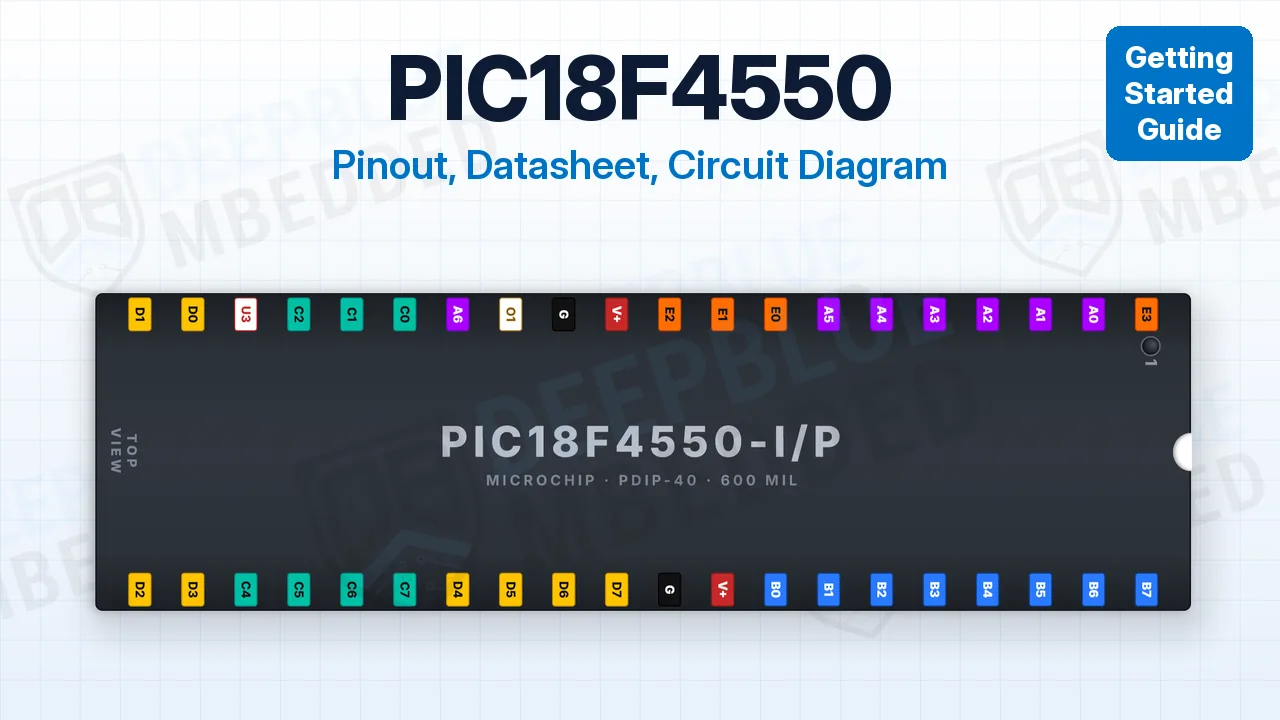
In this guide, you’ll find the PIC18F4550 pinout (pin diagram) for the DIP-40 package, the full pin configuration table (with TQFP-44 and QFN-44 pin numbers), its datasheet, a minimal circuit, and every pin group explained with its reset state and gotchas. Without further ado, let’s get right into it!
The PIC18F4550 is Microchip’s classic USB microcontroller: an 8-bit PIC18 core running up to 48MHz (12 MIPS) with 32KB Flash, 2KB RAM, 256 bytes of EEPROM, and a full-speed USB 2.0 device module with its own transceiver and 3.3v regulator. In the breadboard-friendly PDIP-40 package (PIC18F4550-I/P), it gives you 34 I/O pins, 13 ADC channels, and 2 CCP modules (one of them an enhanced ECCP).
PIC18F4550 Pinout Diagram
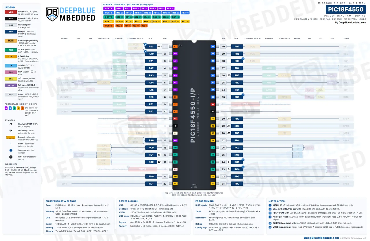
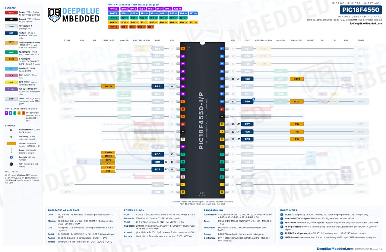
Here is a detailed PIC18F4550 Pinout Diagram with colored labels and legends to help you easily identify the functionalities that each pin can perform. It shows the DIP-40 package from the top, with pin 1 next to the notch and the dot.
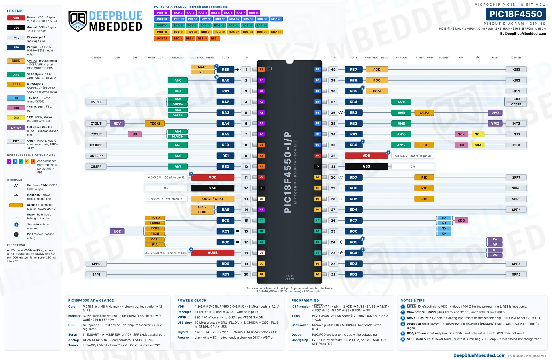
Each row shows the physical pin number, the port bit (RA0, RB5…), and its functions sorted into columns: control and programming, analog, timer/CCP, EUSART, SPI, I2C, USB, and other. The colored tabs inside the chip tell you which port each pin belongs to, the arrows mark the input-only pins (RE3, RC4, and RC5), and the numbered badges point to the notes at the bottom. The same pin diagram also fits the PIC18F4455 and the low-voltage PIC18LF4550.
Buy a PIC18F4550: If you don’t have one yet, you can get the PIC18F4550-I/P DIP-40 chip from Amazon or AliExpress. The DIP package plugs straight into a breadboard, so you can build the minimal circuit below in a few minutes.
Download PIC18F4550 Pinout Diagram (Full Resolution)
The PIC18F4550 DIP-40 pinout diagram in full resolution (5120×3338 px WebP), in one ZIP file. Print it, zoom in, or keep it next to your bench. Please consider supporting my work if it helped you.
PIC18F4550 Datasheet
The PIC18F4550 shares one datasheet with the PIC18F2455, PIC18F2550, and PIC18F4455. Here are the official PIC18F4550 datasheet and errata documents you’ll need, all linked to Microchip’s own servers:
| Document | ID | Revision | What you’ll use it for | Link |
|---|---|---|---|---|
| PIC18F2455/2550/4455/4550 Data Sheet | DS39632 | Rev E (2009) | Pin descriptions (Table 1-3), oscillator and USB clock tables, configuration bits, electrical limits | |
| PIC18F2455/2550/4455/4550 Family Silicon Errata and Data Sheet Clarification | DS80478 | Rev A (2009) | Silicon bugs and datasheet corrections, including the USB regulator default (VREGEN) | |
| Timer1 Module Data Sheet Errata | DS80329 | Rev B (2010) | The Timer1 oscillator and counter issues |
Which document do I need? The datasheet for pin functions, the USB clock setup, and the configuration bits, and the DS80478 errata before you design the USB power path. All of them are listed on the official PIC18F4550 product page, where Microchip shows the PIC18F4550 as In Production and lists the PIC18F45K50 as the newer device. Revision E is still the latest datasheet.
Note: The DS80478 errata corrects the datasheet on the USB regulator: VREGEN is disabled by default (the datasheet text says enabled), so set VREGEN = ON in your configuration bits. It also states that VDD must stay at or above VUSB at all times.
PIC18F4550 Minimal Circuit
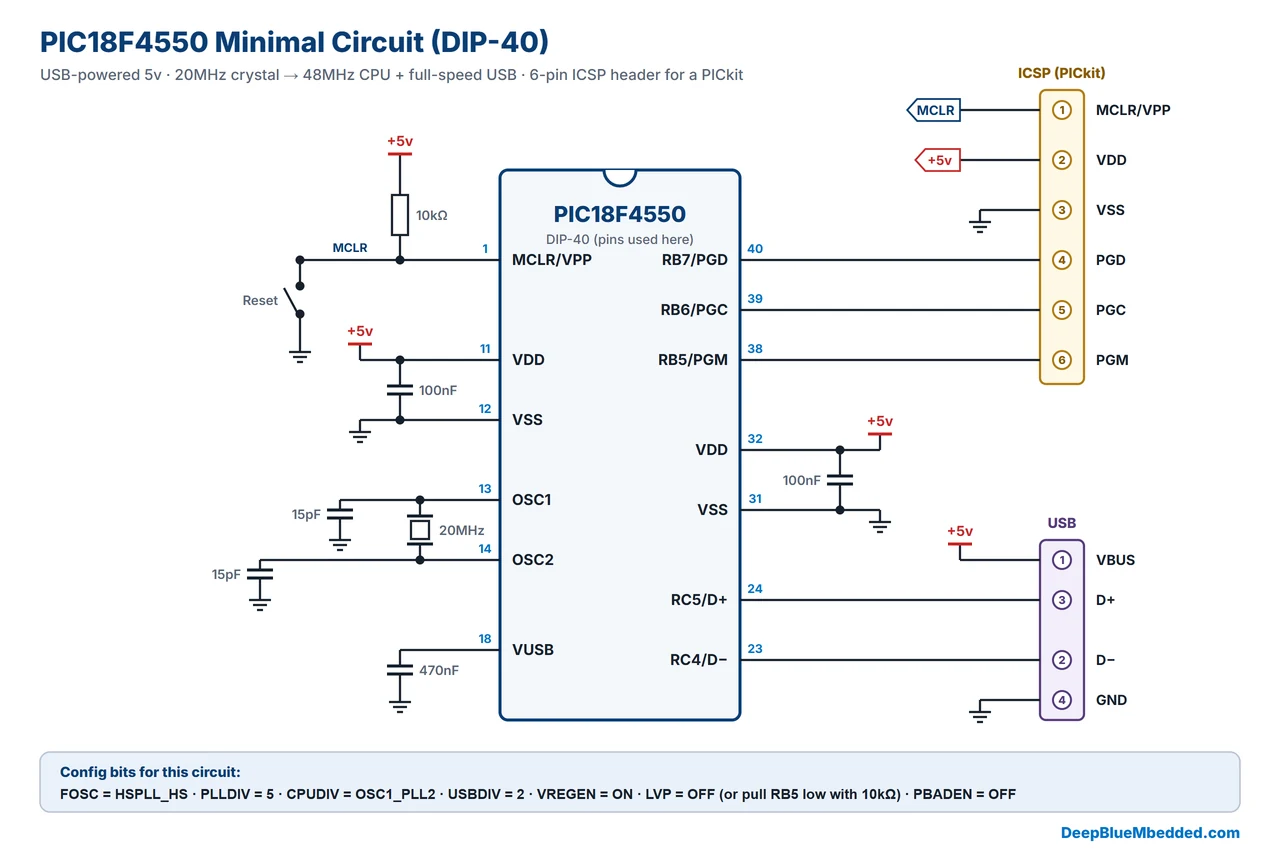
A bare PIC18F4550 needs only a handful of parts to run your code and enumerate on USB: 2 decoupling capacitors, a crystal with 2 load capacitors, a pull-up on MCLR, a capacitor on VUSB, the 6-pin ICSP header for your programmer, and a USB connector. Here is the PIC18F4550 circuit diagram I recommend for a breadboard or a first PCB.
| Part | PIC18F4550 pins | Value | Why |
|---|---|---|---|
| Decoupling capacitor | 11 (VDD) – 12 (VSS) | 100nF ceramic | Keeps the supply clean; place it right at the pins |
| Decoupling capacitor | 32 (VDD) – 31 (VSS) | 100nF ceramic | The second supply pair must be wired and decoupled too |
| Crystal | 13 (OSC1) – 14 (OSC2) | 20MHz (HS) | With the PLL, gives 48MHz for the CPU and the USB module |
| Load capacitors | 13 and 14 to VSS | 15pF each (DS39632E Table 2-2; 22pF also works) | Start the crystal reliably |
| MCLR pull-up | 1 (MCLR) to VDD | 10kΩ | A floating MCLR resets the chip at random |
| Reset button | 1 (MCLR) to VSS | Push button | Optional manual reset |
| VUSB capacitor | 18 (VUSB) to VSS | 470nF ceramic (220nF min) | Stabilizes the internal 3.3v USB regulator |
| ICSP header | 1, 11, 12, 40, 39, 38 | 6-pin, 2.54mm | Connects a PICkit or MPLAB SNAP |
| USB connector | 23 (D−), 24 (D+), VBUS, GND | USB-B or Micro-B | Powers the chip (5v) and carries USB data |
- Power: run the chip from 5v (USB VBUS or a regulated supply). The PIC18F4550 needs at least 4.2v for 48MHz operation, and both VDD/VSS pairs (11/12 and 32/31) must be connected.
- Clock: the 20MHz crystal is the most common choice because the PLL divider (PLLDIV = 5) turns it into the 4MHz the 96MHz USB PLL needs. Any crystal from 4MHz to 24MHz that divides down to 4MHz works too.
- MCLR: a series 100Ω–470Ω resistor or a diode between the pull-up node and a reset capacitor protects your programmer’s VPP voltage. Without a capacitor on MCLR, the plain 10kΩ pull-up is enough.
- Configuration bits: this circuit needs FOSC = HSPLL_HS, PLLDIV = 5, CPUDIV = OSC1_PLL2, USBDIV = 2, VREGEN = ON, LVP = OFF, and PBADEN = OFF. The full block is in the Getting Started section below.
PIC18F4550 Specs
Here are the PIC18F4550 specifications for the DIP-40 package, taken from the DS39632E datasheet.
| Item | PIC18F4550 |
|---|---|
| Core | 8-bit PIC18, 4 clocks per instruction, up to 48MHz (12 MIPS) |
| Program memory | 32KB Flash (16,384 single-word instructions), 100,000 erase/write cycles (typical) |
| Data memory | 2KB SRAM (1KB of it shared with the USB buffers), 256 bytes EEPROM |
| Supply voltage | 4.2v–5.5v for 48MHz (PIC18LF4550: 2.0v–5.5v) |
| I/O | 34 port pins (PORTA–PORTE), including RA6 on OSC2 and the input-only RE3 on MCLR (the device table in the datasheet counts 35 I/O) |
| Current limits | 25mA per I/O pin (sink or source), 200mA total for all ports, 250mA into VDD, 300mA out of VSS |
| USB | Full-speed USB 2.0 device (12Mbps), on-chip transceiver and 3.3v regulator, up to 32 endpoints (16 bidirectional) |
| ADC | 13 channels, 10-bit, external VREF+/VREF− option |
| Timers | Timer0 (8/16-bit), Timer1 and Timer3 (16-bit), Timer2 (8-bit) |
| CCP / PWM | CCP1 as an enhanced ECCP (P1A–P1D, half and full bridge), CCP2 standard |
| Serial | 1x EUSART, 1x MSSP (SPI or I2C), 8-bit Streaming Parallel Port (SPP) |
| Analog extras | 2 comparators, comparator voltage reference, high/low-voltage detect (HLVD) |
| Oscillator | Crystal or resonator up to 25MHz (24MHz with the USB PLL), external clock up to 48MHz, internal 8MHz INTOSC and 31kHz INTRC |
| Programming | ICSP over PGC/PGD (pins 39/40), high-voltage on MCLR/VPP or low-voltage with PGM (pin 38) |
| Packages | PDIP-40 (-I/P), TQFP-44 (-I/PT), QFN-44 (-I/ML) |
Get a PIC18F4550: The PIC18F4550-I/P (DIP-40) is the one I recommend for breadboards. Grab it from Amazon or AliExpress.
PIC18F4550 Specifications Summary
- The PIC18F4550 has 40 pins in DIP-40: 34 I/O, 2 VDD, 2 VSS, OSC1, and VUSB.
- PORTA is RA0–RA6 (RA6 only without a crystal); there is no RA7.
- PORTC has no RC3, and RC4/RC5 are input-only (they are the USB D−/D+ pins).
- RE3 shares pin 1 with MCLR and is input-only (needs MCLRE = OFF).
- 13 ADC channels: AN0–AN4 on PORTA, AN5–AN7 on PORTE, AN8–AN12 on PORTB.
- PWM: CCP1/P1A on RC2 (plus P1B–P1D on RD5–RD7) and CCP2 on RC1 (or RB3).
- EUSART: TX on RC6 (pin 25) and RX on RC7 (pin 26).
- I2C: SDA on RB0 (pin 33) and SCL on RB1 (pin 34); SPI adds SDO on RC7 and SS on RA5.
- USB: D− on pin 23, D+ on pin 24, and a 220nF–470nF capacitor on VUSB (pin 18).
- ICSP: MCLR/VPP pin 1, PGM pin 38, PGC pin 39, PGD pin 40.
- At reset, RA0–RA3, RA5, RE0–RE2, and RB0–RB4 are analog, and RB5 is the LVP programming pin.
- 25mA per pin, 200mA for all ports together; 4.2v–5.5v for 48MHz.
PIC18F4550 Quick Pin Selection Guide
| Use case | Recommended pins | Why |
|---|---|---|
| Serial (UART) | RC6 (TX, pin 25), RC7 (RX, pin 26) | The only EUSART |
| I2C | RB0 (SDA, pin 33), RB1 (SCL, pin 34) | MSSP in I2C mode; add 4.7kΩ pull-ups |
| SPI master | RB1 (SCK), RB0 (SDI), RC7 (SDO), any pin as CS | MSSP in SPI mode; SDO shares RC7 with UART RX |
| PWM | RC2 (CCP1, pin 17), RC1 (CCP2, pin 16) | Hardware PWM from Timer2 |
| Motor H-bridge | RC2/P1A, RD5/P1B, RD6/P1C, RD7/P1D | ECCP half/full-bridge with dead band |
| Analog input | RA0–RA3 (AN0–AN3) | Analog at reset, no other function in the way |
| External interrupt | RB0 (INT0), RB1 (INT1), RB2 (INT2) | Edge-triggered interrupts |
| Button / keypad | RB4–RB7 (interrupt-on-change) | Internal weak pull-ups on PORTB (RBPU) |
| USB | RC4 (D−, pin 23), RC5 (D+, pin 24) | Fixed USB pins, with the cap on VUSB |
| LEDs and general outputs | PORTD (RD0–RD7) | Digital at reset and 8 bits in a row |
| Character LCD (4-bit) | PORTD | No analog setup needed |
PIC18F4550 Pins to Use With Caution
| Pin | Reason | What to do |
|---|---|---|
| RB5 / PGM (38) | LVP is ON by default: a floating or high RB5 puts the chip into programming mode (random resets or freezes) | Set LVP = OFF, or pull RB5 low with 10kΩ |
| RB0–RB4 (33–37) | PBADEN = ON by default makes them analog, so they read 0 as digital inputs | PBADEN = OFF or ADCON1 = 0x0F |
| RA0–RA3, RA5, RE0–RE2 | Analog at reset | ADCON1 = 0x0F for all-digital |
| RC4, RC5 (23, 24) | Input-only (no TRISC bit), and digital only with the USB module off | Use them for USB, or as inputs only |
| RC3 | Doesn’t exist on this chip | Don’t look for it in TRISC |
| MCLR / RE3 (1) | Resets the chip when low; sees 9v–13.25v during programming | 10kΩ pull-up; never connect it straight to other circuits |
| VUSB (18) | A regulator output, not a supply input | 220nF–470nF to ground; never feed 5v into it |
| OSC1, OSC2 (13, 14) | Taken by the crystal | Leave them to the crystal |
| RB6, RB7 (39, 40) | PGC/PGD for ICSP and debugging | Keep loads light (no low-value resistors or big capacitors) |
| RC7 (26) | Shared by UART RX and SPI SDO | Pick one of them for your design |
PIC18F4550 Pin Diagram Explained
The 40 pins in the PIC18F4550 pin diagram are divided into the following groups based on the hardware functionality they’re used for:
- 6x Power Pins (2 VDD, 2 VSS, VUSB, and MCLR)
- 34x I/O Pins (PORTA–PORTE)
- 13x ADC Analog Input Pins
- 6x PWM Pins (CCP1/ECCP and CCP2)
- 1x EUSART (UART) Port
- 1x MSSP Port (SPI or I2C)
- 1x Full-Speed USB Port
- 1x Streaming Parallel Port (SPP)
- 2x Oscillator Pins
- 5x ICSP Programming Pins
We’ll discuss each pin group in the following sections one by one in more detail.
PIC18F4550 Power Pins
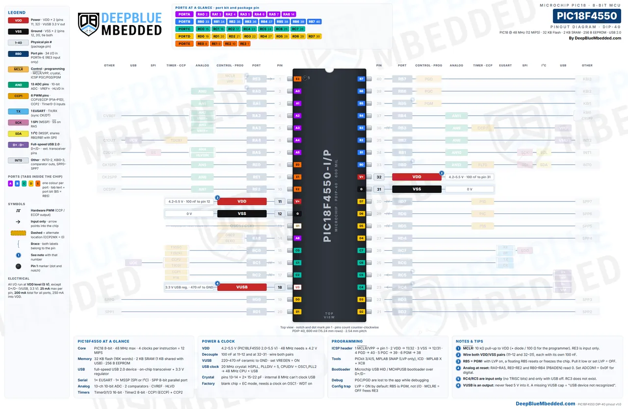
The PIC18F4550 has 2 VDD pins (11 and 32) and 2 VSS pins (12 and 31), and you must connect all four, each pair with its own 100nF capacitor. Pin 18 (VUSB) is the output of the internal 3.3v USB regulator.
| Pin | Name | Function | Notes |
|---|---|---|---|
| 11, 32 | VDD | Positive supply | 4.2v–5.5v (2.0v–5.5v on the PIC18LF4550); 250mA max into VDD |
| 12, 31 | VSS | Ground | 300mA max out of VSS |
| 18 | VUSB | USB transceiver supply (3.3v) | Regulator output with VREGEN = ON; 220nF–470nF to ground |
| 1 | MCLR/VPP | Reset / programming voltage | 10kΩ pull-up to VDD |
The PIC18F4550 runs at 48MHz from 4.2v to 5.5v. Below 4.2v, you need the PIC18LF4550 and a lower clock. When VDD is below about 4v, the internal regulator can’t make 3.3v for USB, so you turn VREGEN off and feed 3.0v–3.6v into VUSB from an external regulator instead (and VDD must never be lower than VUSB, per the errata).
Note: Wire both VDD/VSS pairs. The 28-pin PIC18F2550 has a single VDD pin, and people moving to the 40-pin chip often leave pin 32 or pin 31 open. The chip may even seem to work, until a heavy load or USB activity makes it reset.
PIC18F4550 I/O Ports (PORTA–PORTE)
The PIC18F4550 has 5 I/O ports with 34 I/O pins in total: PORTA (7), PORTB (8), PORTC (7), PORTD (8), and PORTE (4, including the input-only RE3). Every pin works at the VDD level (5v) and can sink or source 25mA, with 200mA for all ports together.
| Port | Pins (DIP) | Bits | Reset state | Notes |
|---|---|---|---|---|
| PORTA | 2–7, 14 | RA0–RA6 | RA0–RA3, RA5 analog; RA4 digital input | RA6 only in ECIO/INTIO modes (pin 14 is OSC2 with a crystal); RA4 is a full CMOS output here |
| PORTB | 33–40 | RB0–RB7 | RB0–RB4 analog (PBADEN = ON); RB5 = PGM (LVP = ON) | Weak pull-ups (RBPU), INT0–INT2, interrupt-on-change on RB4–RB7 |
| PORTC | 15–17, 23–26 | RC0–RC2, RC4–RC7 | Digital inputs | No RC3; RC4/RC5 are input-only USB pins |
| PORTD | 19–22, 27–30 | RD0–RD7 | Digital inputs | Schmitt trigger inputs, optional pull-ups (RDPU), SPP data bus |
| PORTE | 8–10, 1 | RE0–RE3 | RE0–RE2 analog; RE3 = MCLR | RE3 is input-only and needs MCLRE = OFF |
Each port has the usual three registers: TRISx sets the direction (1 = input, 0 = output), PORTx reads the pins, and LATx writes the output latch. Write outputs through LATx, so a read-modify-write on PORTx never flips another pin by mistake.
Note: Most “my input always reads 0” problems on the PIC18F4550 come from the analog default: 13 pins are analog at reset. Add ADCON1 = 0x0F; at the start of main() (and #pragma config PBADEN = OFF) to make every pin digital. The comparators are already off at reset (CMCON = 0x07).
PIC18F4550 Interrupt Pins
PIC18F4550 External Interrupt Pins: INT0 on RB0 (pin 33), INT1 on RB1 (pin 34), and INT2 on RB2 (pin 35). RB4–RB7 (pins 37–40) add an interrupt-on-change on any edge, which is handy for a keypad or buttons with PORTB’s internal pull-ups.
Learn more in our PIC GPIO Tutorial.
Also Read
PIC18F4550 ADC Pins
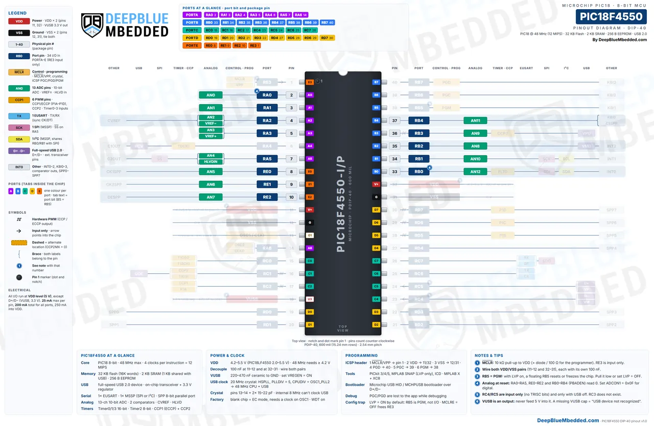
The PIC18F4550 has a 10-bit ADC with 13 analog input channels (AN0–AN12) in the DIP-40 package. AN0–AN3 on RA0–RA3 are the easiest ones to use, because nothing else competes for those pins.
| Channel | Pin (DIP) | Port | Also |
|---|---|---|---|
| AN0 | 2 | RA0 | – |
| AN1 | 3 | RA1 | – |
| AN2 | 4 | RA2 | VREF−, CVREF |
| AN3 | 5 | RA3 | VREF+ |
| AN4 | 7 | RA5 | SS, HLVDIN, C2OUT |
| AN5 | 8 | RE0 | CK1SPP |
| AN6 | 9 | RE1 | CK2SPP |
| AN7 | 10 | RE2 | OESPP |
| AN8 | 35 | RB2 | INT2 |
| AN9 | 36 | RB3 | CCP2 (alt) |
| AN10 | 34 | RB1 | INT1, SCK, SCL |
| AN11 | 37 | RB4 | KBI0, CSSPP |
| AN12 | 33 | RB0 | INT0, SDI, SDA |
The PCFG3:PCFG0 bits in ADCON1 select how many channels are analog, always counting up from AN0 (you can’t pick AN5 alone, for example). ADCON1 = 0x0E keeps only AN0 analog, and 0x0F makes everything digital. By default the ADC reference is VDD and VSS; RA3 and RA2 can bring in an external VREF+ and VREF−.
Note: Note that the channel numbers on PORTB aren’t in pin order (AN12 is on RB0 and AN10 is on RB1). And since PBADEN makes RB0–RB4 analog at reset, the I2C pins (RB0/RB1) won’t work until you make them digital.
Learn more in our PIC ADC Tutorial.
Also Read
PIC18F4550 PWM Pins (CCP/ECCP)
PIC18F4550 Default PWM Pins: CCP1 on RC2 (pin 17) and CCP2 on RC1 (pin 16). Both use Timer2 as the time base, so they share one PWM frequency, with up to 10-bit duty-cycle resolution.
| Signal | Pin (DIP) | Port | Notes |
|---|---|---|---|
| CCP1 / P1A | 17 | RC2 | Capture, compare, PWM; ECCP output A |
| P1B | 28 | RD5 | ECCP half/full-bridge output B |
| P1C | 29 | RD6 | ECCP full-bridge output C |
| P1D | 30 | RD7 | ECCP full-bridge output D |
| CCP2 | 16 | RC1 | Default location (CCP2MX = ON) |
| CCP2 (alternate) | 36 | RB3 | With CCP2MX = OFF |
| FLT0 | 33 | RB0 | ECCP auto-shutdown input |
On the 40-pin chip, CCP1 is an Enhanced CCP (ECCP): it can drive a half-bridge (P1A/P1B) or a full H-bridge (P1A–P1D) with programmable dead band and an auto-shutdown on the FLT0 pin, which makes it a good fit for DC motor control. The timer clock inputs are on RA4 (T0CKI) and RC0 (T13CKI for Timer1 and Timer3), and the 32.768kHz Timer1 oscillator goes on RC0/RC1.
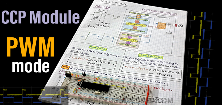
Learn more in our PIC PWM Tutorial.
Also Read
PIC18F4550 UART Pins (EUSART)
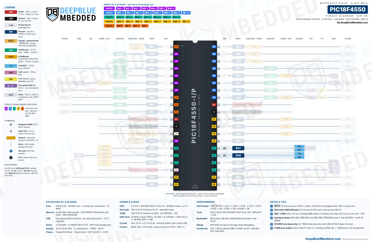
PIC18F4550 UART Pins: TX on RC6 (pin 25) and RX on RC7 (pin 26). The PIC18F4550 has one EUSART, which also supports synchronous mode (CK/DT), auto-baud detection, and a 16-bit baud rate generator.
| Signal | Pin (DIP) | Port | Notes |
|---|---|---|---|
| TX / CK | 25 | RC6 | Transmit (async) or clock (sync) |
| RX / DT | 26 | RC7 | Receive (async) or data (sync); also SPI SDO |
Set TRISC6 = 1 and TRISC7 = 1 (inputs) and let the EUSART take over both pins when SPEN is set. The baud rate is calculated from the CPU clock, so it’s only right if your configuration bits really give you the Fosc you think (see the “4x too slow” problem below).
Note: RC7 is both the UART RX and the SPI SDO pin. You can’t use the EUSART receiver and the MSSP as an SPI master at the same time. If you need both, use I2C for the second peripheral or a software UART.
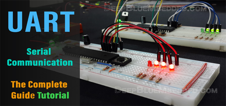
Learn more in our PIC UART Tutorial.
Also Read
PIC18F4550 SPI and I2C Pins (MSSP)
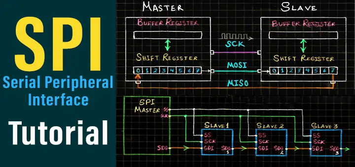
The PIC18F4550 has one MSSP (Master Synchronous Serial Port) module that works either as SPI or as I2C, not both at once. The clock (SCK/SCL) is on RB1 (pin 34) and the data input (SDI/SDA) is on RB0 (pin 33) in both modes.
PIC18F4550 SPI Pins
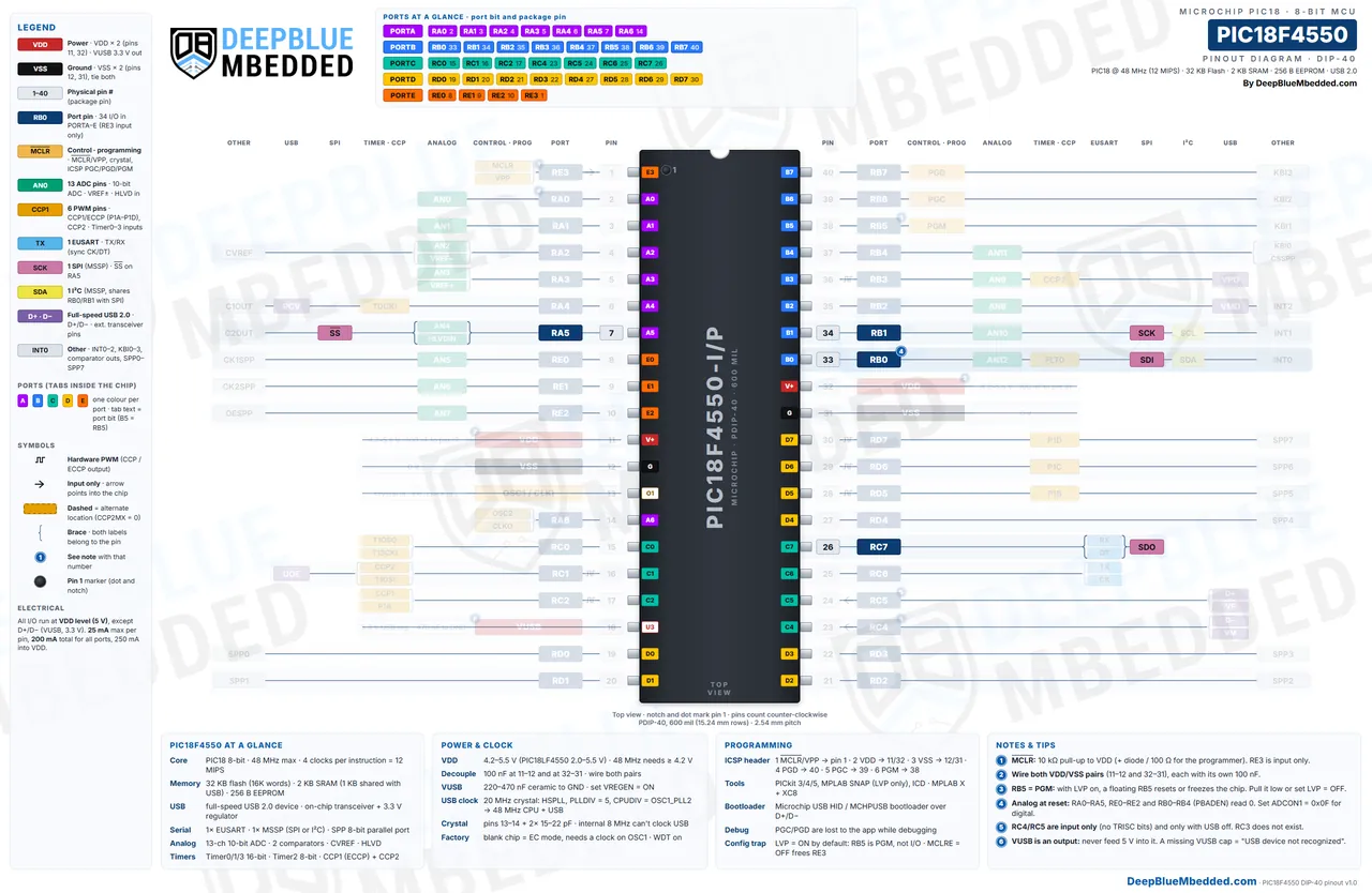
PIC18F4550 SPI Pins: SCK RB1 (pin 34), SDI RB0 (pin 33), SDO RC7 (pin 26), and SS RA5 (pin 7, slave mode only).
| Signal | Pin (DIP) | Port | Direction (master) |
|---|---|---|---|
| SCK | 34 | RB1 | Output (TRISB1 = 0) |
| SDI | 33 | RB0 | Input (TRISB0 = 1) |
| SDO | 26 | RC7 | Output (TRISC7 = 0) |
| SS | 7 | RA5 | Slave select input (slave mode); use any pin as CS in master mode |
Learn more in our PIC SPI Tutorial.
Also Read
PIC18F4550 I2C Pins
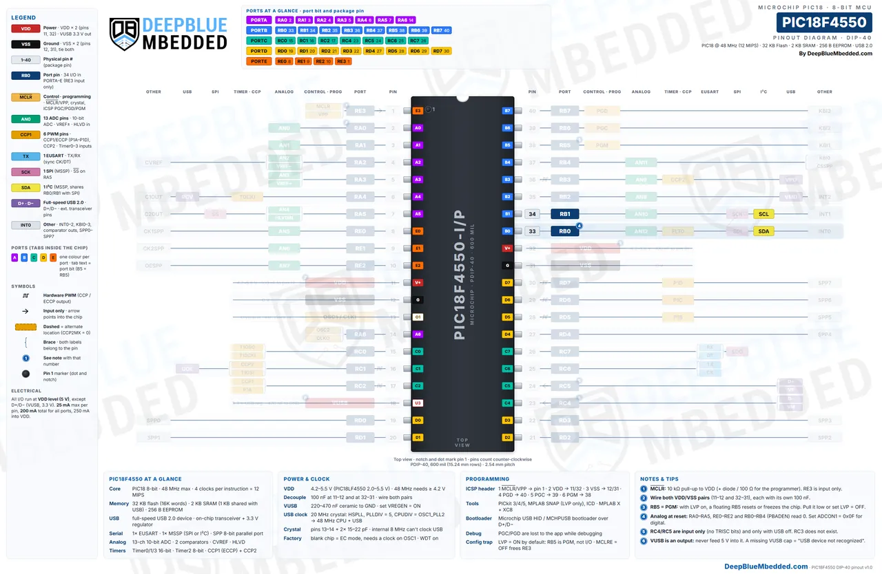
PIC18F4550 I2C Pins: SDA on RB0 (pin 33) and SCL on RB1 (pin 34). Set both pins as inputs (TRISB0 = TRISB1 = 1), make them digital (ADCON1 = 0x0F), and add 4.7kΩ pull-up resistors to VDD.
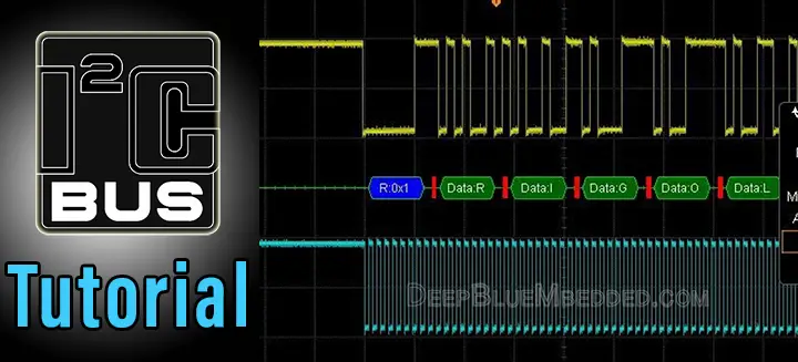
There are so many modules and sensors that we can interface with the PIC18F4550 using the I2C bus, which include: I2C LCD adapters (PCF8574), EEPROM memory chips, RTC clock modules (DS3231), MPU6050 IMU sensors, OLED display screens, and much more.
Learn more in our PIC I2C Tutorial.
Also Read
PIC18F4550 USB Pins
PIC18F4550 USB Pins: D− on RC4 (pin 23) and D+ on RC5 (pin 24), with the internal 3.3v regulator output on VUSB (pin 18). The full-speed USB 2.0 device module has its own transceiver, so you connect D+ and D− straight to the USB connector, with no resistors.
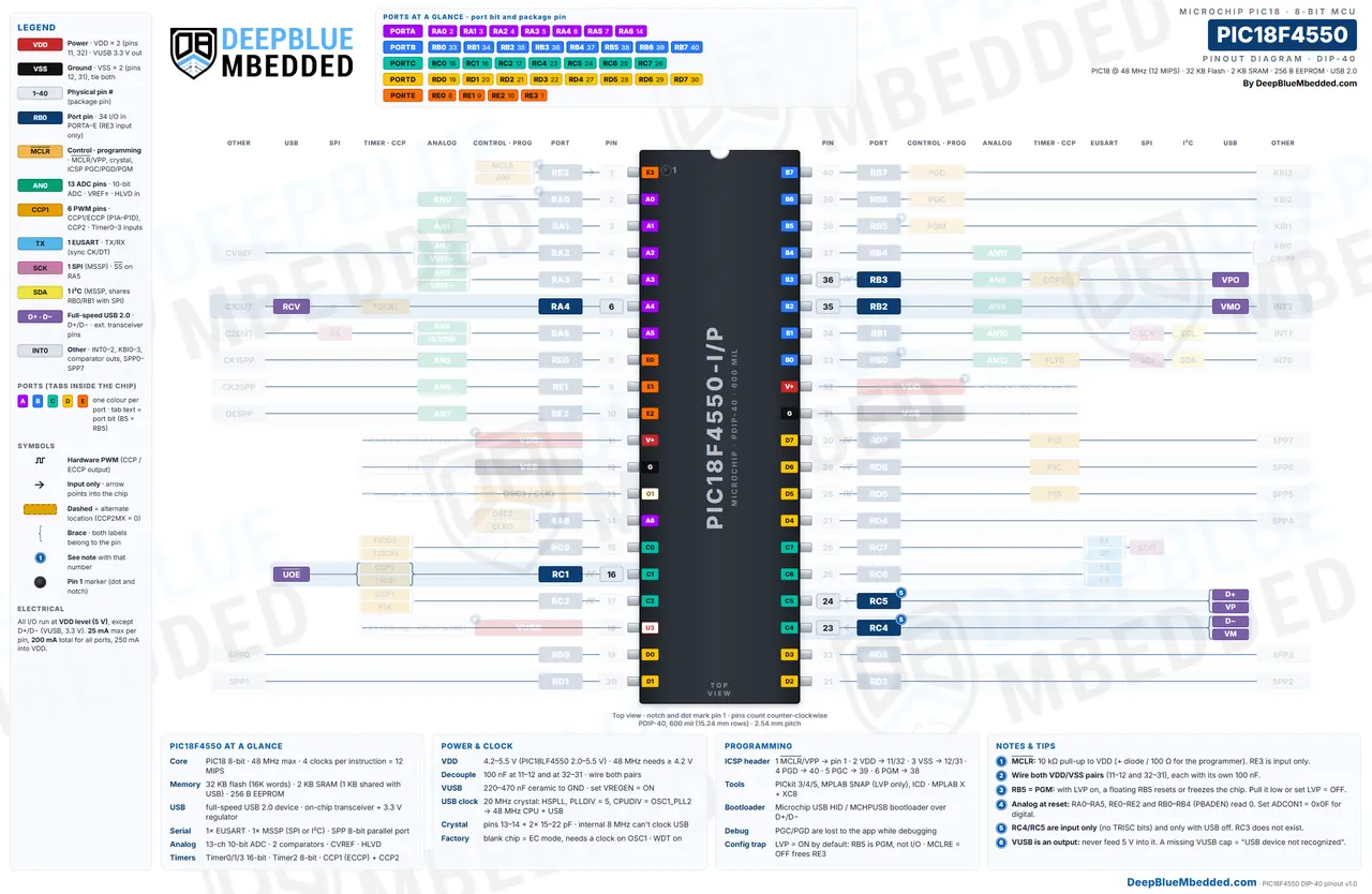
| Pin (DIP) | Signal | Function |
|---|---|---|
| 23 | RC4 / D− / VM | USB data − (or VM input from an external transceiver) |
| 24 | RC5 / D+ / VP | USB data + (or VP input from an external transceiver) |
| 18 | VUSB | 3.3v regulator output for the transceiver and pull-up; 220nF–470nF to ground |
| 16 | RC1 / UOE | External transceiver output enable |
| 6 | RA4 / RCV | External transceiver receive input |
| 35, 36 | RB2 / VMO, RB3 / VPO | External transceiver outputs |
Full-speed USB needs a 48MHz USB clock, which comes from the 96MHz PLL divided by 2. The PLL input must be exactly 4MHz, so the PLLDIV setting has to match your crystal (see the oscillator section). The internal 8MHz oscillator can run the CPU but can’t clock full-speed USB, so a USB design always needs a crystal or an external clock.
Note: RC4 and RC5 have no TRISC bits: they can never be outputs. With the USB module off (UCON.USBEN = 0 and UCFG.UTRDIS = 1), they work as digital inputs only. An LED on RC4 or RC5 will never light up.
PIC18F4550 SPP Pins (Streaming Parallel Port)
The PIC18F4550 has an 8-bit Streaming Parallel Port (SPP) on PORTD, made for streaming data between the USB endpoints and an external parallel device (an FPGA, a camera, or a memory) with little CPU work. It exists only on the 40/44-pin chips (PIC18F4455/4550).
| Signal | Pins (DIP) | Port | Function |
|---|---|---|---|
| SPP0–SPP3 | 19–22 | RD0–RD3 | Data bus, bits 0–3 |
| SPP4–SPP7 | 27–30 | RD4–RD7 | Data bus, bits 4–7 |
| CK1SPP | 8 | RE0 | Clock 1 output |
| CK2SPP | 9 | RE1 | Clock 2 output |
| OESPP | 10 | RE2 | Output enable |
| CSSPP | 37 | RB4 | Chip select |
PIC18F4550 Oscillator Pins (Crystal and USB Clock)
PIC18F4550 Oscillator Pins: OSC1/CLKI on pin 13 and OSC2/CLKO on pin 14. For USB, the crystal is divided down to 4MHz by PLLDIV, multiplied to 96MHz by the PLL, and then divided by 2 for the USB module (48MHz) and by CPUDIV for the CPU.
| Crystal | PLLDIV | Clock mode | CPUDIV for 48MHz CPU | XC8 setting |
|---|---|---|---|---|
| 4MHz | ÷1 | HSPLL_HS | 96MHz ÷ 2 | PLLDIV = 1 |
| 8MHz | ÷2 | HSPLL_HS | 96MHz ÷ 2 | PLLDIV = 2 |
| 12MHz | ÷3 | HSPLL_HS | 96MHz ÷ 2 | PLLDIV = 3 |
| 16MHz | ÷4 | HSPLL_HS | 96MHz ÷ 2 | PLLDIV = 4 |
| 20MHz | ÷5 | HSPLL_HS | 96MHz ÷ 2 | PLLDIV = 5 |
| 24MHz | ÷6 | HSPLL_HS | 96MHz ÷ 2 | PLLDIV = 6 |
With the PLL on, the CPUDIV names are confusing: CPUDIV = OSC1_PLL2 means “96MHz ÷ 2 = 48MHz“, OSC2_PLL3 means 32MHz, OSC3_PLL4 means 24MHz, and OSC4_PLL6 means 16MHz. Without the PLL (HS mode), the same setting would divide the crystal frequency instead. A 40MHz or 48MHz source works only as an external oscillator (EC modes, PLLDIV ÷10 or ÷12), not as a crystal.
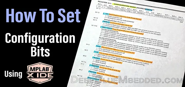
Note: A blank PIC18F4550 starts in EC mode (it expects an external clock on OSC1) with the watchdog timer on. With only a crystal fitted, it won’t run until you program the configuration bits. The internal 8MHz INTOSC (with 31kHz INTRC) is fine for non-USB projects.
Learn more in our PIC Configuration Bits Tutorial.
Also Read
PIC18F4550 ICSP Programming Pins
The PIC18F4550 is programmed over ICSP (In-Circuit Serial Programming) with 5 signals: MCLR/VPP (pin 1), PGC (pin 39), PGD (pin 40), VDD, and VSS, plus PGM (pin 38) for low-voltage programming. Here’s how the standard 6-pin PICkit header maps to the chip:
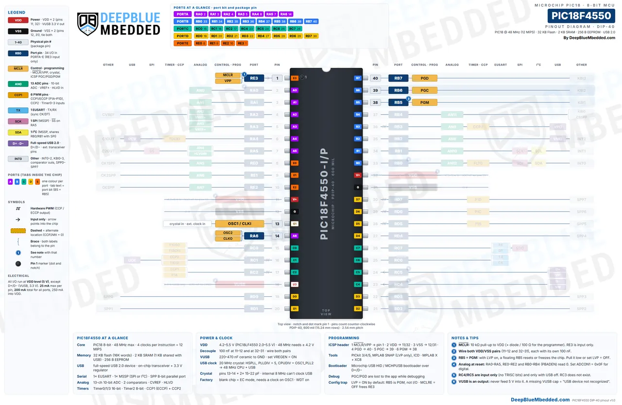
| ICSP header pin | Signal | PIC18F4550 pin (DIP) |
|---|---|---|
| 1 | MCLR/VPP | 1 |
| 2 | VDD | 11 (and 32) |
| 3 | VSS | 12 (and 31) |
| 4 | PGD | 40 (RB7) |
| 5 | PGC | 39 (RB6) |
| 6 | PGM / LVP | 38 (RB5), only for low-voltage programming |
- PICkit 3/4/5 and MPLAB ICD: high-voltage programming (VPP of 9v–13.25v on MCLR), with MPLAB X IDE and the XC8 compiler. Pin 6 of the header can stay unconnected.
- MPLAB SNAP: it can’t generate the high VPP voltage, so it programs the PIC18F4550 in low-voltage mode only. That means LVP must stay ON, and RB5 belongs to the programmer.
- USB HID bootloader: many projects program Microchip’s USB HID bootloader once over ICSP, then load new firmware over USB with no programmer.
- Debugging takes PGC and PGD (and a little RAM and Flash), so keep those pins free while you debug.
Note: With the default LVP = ON, RB5 is the PGM pin, not an I/O. If RB5 floats or goes high, the chip enters programming mode and looks like it resets or freezes at random. Set LVP = OFF when you use a PICkit, or pull RB5 low with a 10kΩ resistor.
Getting Started With PIC18F4550
To program the PIC18F4550, install MPLAB X IDE and the free MPLAB XC8 compiler (the old MPLAB C18 compiler is legacy), build the minimal circuit, and connect a PICkit to the ICSP header. Here’s a complete XC8 example for the 20MHz crystal circuit: the configuration bits for 48MHz and USB, PORTB made digital, and an LED blinking on RD0.
|
1 2 3 4 5 6 7 8 9 10 11 12 13 14 15 16 17 |
// PIC18F4550, 20MHz crystal -> 48MHz CPU and USB clock #pragma config PLLDIV = 5, CPUDIV = OSC1_PLL2, USBDIV = 2 #pragma config FOSC = HSPLL_HS, FCMEN = OFF, IESO = OFF #pragma config PWRT = ON, BOR = ON, VREGEN = ON #pragma config WDT = OFF, MCLRE = ON, PBADEN = OFF, LVP = OFF, XINST = OFF #include <xc.h> #define _XTAL_FREQ 48000000 void main(void) { ADCON1 = 0x0F; // all pins digital (RA, RB0-RB4, RE are analog at reset) TRISDbits.TRISD0 = 0; // RD0 (pin 19) as output while (1) { LATDbits.LATD0 ^= 1; // toggle the LED __delay_ms(500); } } |
The gotcha in this code is the ADCON1 = 0x0F; line: without it (or PBADEN = OFF), RB0–RB4 and the PORTA/PORTE analog pins read 0 as digital inputs. Learn more about the configuration bits and the rest of the peripherals in our PIC Microcontrollers Programming Tutorials series, and for a ready-made board, check out the PIC18F Development Board.
PIC18F4550 Common Problems & Fixes
Why does my PIC18F4550 reset or freeze at random? Usually RB5 is floating while LVP is ON (the default), so the chip enters programming mode. Set LVP = OFF or pull RB5 low (picbasic.co.uk). A missing MCLR pull-up does the same.
Why do my PORTB inputs always read 0? RB0–RB4 are analog at reset (PBADEN = ON), along with RA0–RA3, RA5, and RE0–RE2. Write ADCON1 = 0x0F; or set PBADEN = OFF.
Why won’t my LED on RC4 or RC5 light up? RC4 and RC5 are input-only USB pins with no TRISC bits (CCS forum). Move the LED to another pin.
Why does Windows say “USB device not recognized”? Check the 220nF–470nF capacitor on VUSB (pin 18), set VREGEN = ON (it’s off by default, per errata DS80478), match PLLDIV to your crystal, and check that D+ (pin 24) and D− (pin 23) aren’t swapped (picbasic.co.uk).
Why does my code run 4x too slow, or my UART baud rate come out wrong? The configuration bits don’t give the clock your code assumes: a wrong FOSC (HS instead of HSPLL_HS), PLLDIV, or CPUDIV. With a 20MHz crystal, use FOSC = HSPLL_HS, PLLDIV = 5, CPUDIV = OSC1_PLL2 for 48MHz (picbasic.co.uk).
Why doesn’t my brand-new chip run with a crystal? A blank PIC18F4550 defaults to EC (external clock) mode with the watchdog on. Program the configuration bits first.
Can I use RA4 as an open-drain output like on the PIC16F877A? No. On the PIC18F4550, RA4 is a full CMOS output that drives both high and low.
PIC18F4550 vs PIC18F4455 vs PIC18F2550 vs PIC18F45K50 vs PIC16F877A
The PIC18F4550 has 4 close relatives that students and makers compare it with. Here’s how they differ:
| Feature | PIC18F4550 | PIC18F4455 | PIC18F2550 | PIC18F45K50 | PIC16F877A |
|---|---|---|---|---|---|
| Pins (DIP) | 40 | 40 | 28 | 40 | 40 |
| Pin compatible with the PIC18F4550 | – | Yes, same pins | No (28-pin map) | Yes | Same footprint, different functions |
| Flash | 32KB | 24KB | 32KB | 32KB | 14KB |
| Max CPU clock | 48MHz | 48MHz | 48MHz | 48MHz | 20MHz |
| USB | Full speed | Full speed | Full speed | Full speed, crystal-free option | No |
| ADC | 13-ch 10-bit | 13-ch 10-bit | 10-ch 10-bit | More channels, ANSELx registers | 8-ch 10-bit |
| ECCP / SPP | Yes / Yes | Yes / Yes | No / No | Yes / No | No / No (PSP instead) |
| LVP pin | RB5 | RB5 | RB5 | RB5 | RB3 |
The PIC18F4455 is the same chip with less Flash, so this whole article applies to it. The PIC18F2550 is the 28-pin version (no PORTD, no PORTE except RE3, a single VDD pin), so its pin map is different. The PIC18F45K50 is Microchip’s newer, pin-compatible replacement: it can run USB from its internal oscillator without a crystal and works at lower voltages, but its configuration bits and analog registers (ANSELx instead of ADCON1) differ, so the code needs porting. The PIC16F877A is the classic 40-pin teaching chip with no USB and a slower core.
PIC18F4550 Pin Configuration
Here is the complete PIC18F4550 pin configuration for all 3 packages: the DIP-40 pin number, its TQFP-44 and QFN-44 numbers, every function, the pin type and reset state, and a short description. On the DIP-40, pin 1 is top-left next to the notch, and the pins count counter-clockwise (pin 40 is opposite pin 1).
Click to expand the full pin table (42 pins)
| DIP-40 | TQFP-44 | QFN-44 | Pin name | Functions | Type / reset state | Description |
|---|---|---|---|---|---|---|
| 1 | 18 | 18 | MCLR/VPP/RE3 | MCLR (reset, active low), VPP, RE3 | Input · MCLR at reset | Master clear reset with a 10kΩ pull-up to VDD, the 9v–13.25v programming voltage input, or the RE3 digital input when MCLRE = OFF. |
| 2 | 19 | 19 | RA0 | AN0 | I/O · analog at reset | Analog input AN0; set ADCON1 = 0x0F to use it as a digital pin. |
| 3 | 20 | 20 | RA1 | AN1 | I/O · analog at reset | Analog input AN1; digital only after ADCON1 is set. |
| 4 | 21 | 21 | RA2 | AN2, VREF−, CVREF | I/O · analog at reset | Analog input AN2, the ADC negative reference input, or the comparator reference voltage output. |
| 5 | 22 | 22 | RA3 | AN3, VREF+ | I/O · analog at reset | Analog input AN3 or the ADC positive reference input. |
| 6 | 23 | 23 | RA4 | T0CKI, C1OUT, RCV | I/O · digital input | Timer0 clock input and comparator 1 output; a full CMOS output on this chip (not open drain), with a Schmitt trigger input. |
| 7 | 24 | 24 | RA5 | AN4, SS, HLVDIN, C2OUT | I/O · analog at reset | Analog input AN4, the SPI slave select input, the HLVD input, or comparator 2 output. |
| 8 | 25 | 25 | RE0 | AN5, CK1SPP | I/O · analog at reset | Analog input AN5 or the SPP clock 1 output. |
| 9 | 26 | 26 | RE1 | AN6, CK2SPP | I/O · analog at reset | Analog input AN6 or the SPP clock 2 output. |
| 10 | 27 | 27 | RE2 | AN7, OESPP | I/O · analog at reset | Analog input AN7 or the SPP output enable. |
| 11 | 28 | 7, 8 | VDD | Supply | Power | Positive supply (4.2v–5.5v for 48MHz); decouple with 100nF to pin 12. |
| 12 | 29 | 6 | VSS | Ground | Power | Ground for the pin 11 supply pair. |
| 13 | 30 | 32 | OSC1/CLKI | Crystal in, external clock in | Oscillator | Crystal or resonator input, or the external clock input (EC modes). |
| 14 | 31 | 33 | OSC2/CLKO/RA6 | Crystal out, CLKO, RA6 | Oscillator · CLKO at reset | Crystal output, the Fosc/4 clock output in EC mode, or the RA6 I/O in ECIO and INTIO modes. |
| 15 | 32 | 34 | RC0 | T1OSO, T13CKI | I/O · digital input | Timer1 oscillator output, or the Timer1/Timer3 external clock input. |
| 16 | 35 | 35 | RC1 | T1OSI, CCP2, UOE | I/O · digital input | Timer1 oscillator input, the default CCP2 PWM output (CCP2MX = ON), or the external USB transceiver output enable. |
| 17 | 36 | 36 | RC2 | CCP1, P1A | I/O · digital input | CCP1 capture/compare/PWM, and the ECCP P1A output. |
| 18 | 37 | 37 | VUSB | USB 3.3v regulator | Power (output) | Internal 3.3v USB regulator output: put 220nF–470nF to ground and never feed 5v into it. |
| 19 | 38 | 38 | RD0 | SPP0 | I/O · digital input | PORTD bit 0 and SPP data bit 0. |
| 20 | 39 | 39 | RD1 | SPP1 | I/O · digital input | PORTD bit 1 and SPP data bit 1. |
| 21 | 40 | 40 | RD2 | SPP2 | I/O · digital input | PORTD bit 2 and SPP data bit 2. |
| 22 | 41 | 41 | RD3 | SPP3 | I/O · digital input | PORTD bit 3 and SPP data bit 3. |
| 23 | 42 | 42 | RC4/D−/VM | D−, VM | Input only | USB D− line; a digital input only (no TRISC bit) and only when the USB module is off. |
| 24 | 43 | 43 | RC5/D+/VP | D+, VP | Input only | USB D+ line; a digital input only (no TRISC bit) and only when the USB module is off. |
| 25 | 44 | 44 | RC6 | TX, CK | I/O · digital input | EUSART transmit (asynchronous) or clock (synchronous). |
| 26 | 1 | 1 | RC7 | RX, DT, SDO | I/O · digital input | EUSART receive or data, and also the SPI data output, so the UART RX and SPI master can’t be used together. |
| 27 | 2 | 2 | RD4 | SPP4 | I/O · digital input | PORTD bit 4 and SPP data bit 4. |
| 28 | 3 | 3 | RD5 | SPP5, P1B | I/O · digital input | SPP data bit 5 and the ECCP P1B PWM output. |
| 29 | 4 | 4 | RD6 | SPP6, P1C | I/O · digital input | SPP data bit 6 and the ECCP P1C PWM output. |
| 30 | 5 | 5 | RD7 | SPP7, P1D | I/O · digital input | SPP data bit 7 and the ECCP P1D PWM output. |
| 31 | 6 | 30, 31 | VSS | Ground | Power | Ground for the pin 32 supply pair. |
| 32 | 7 | 28, 29 | VDD | Supply | Power | Second positive supply pin; wire it and decouple it with 100nF to pin 31. |
| 33 | 8 | 9 | RB0 | AN12, INT0, FLT0, SDI, SDA | I/O · analog at reset (PBADEN) | External interrupt INT0, the ECCP fault input, SPI data in, and the I2C SDA line. |
| 34 | 9 | 10 | RB1 | AN10, INT1, SCK, SCL | I/O · analog at reset (PBADEN) | External interrupt INT1, and the SPI clock or I2C SCL line. |
| 35 | 10 | 11 | RB2 | AN8, INT2, VMO | I/O · analog at reset (PBADEN) | External interrupt INT2 and analog input AN8. |
| 36 | 11 | 12 | RB3 | AN9, CCP2, VPO | I/O · analog at reset (PBADEN) | Analog input AN9, or the CCP2 PWM output when CCP2MX = OFF. |
| 37 | 14 | 14 | RB4 | AN11, KBI0, CSSPP | I/O · analog at reset (PBADEN) | Analog input AN11, an interrupt-on-change pin, and the SPP chip select. |
| 38 | 15 | 15 | RB5 | KBI1, PGM | I/O · PGM at reset (LVP) | Interrupt-on-change pin, and the low-voltage programming pin while LVP = ON (the default). |
| 39 | 16 | 16 | RB6 | KBI2, PGC | I/O · digital input | Interrupt-on-change pin and the ICSP programming clock. |
| 40 | 17 | 17 | RB7 | KBI3, PGD | I/O · digital input | Interrupt-on-change pin and the ICSP programming data line. |
| – | 12, 13, 33, 34 | – | NC / ICPORTS | ICCK/ICPGC, ICDT/ICPGD, ICRST/ICVPP, ICPORTS | TQFP-44 only | A dedicated debug port when ICPRT = ON; not connected otherwise. |
| – | – | 13 | NC | – | QFN-44 only | Not connected. |
The TQFP-44 and QFN-44 packages have the same functions as the DIP-40, just on different pin numbers. On the QFN-44, the supply is split over more pins (7, 8, 28, and 29 are VDD; 6, 30, and 31 are VSS), so connect every one of them.
Wrap Up
To conclude this guide article, the PIC18F4550 is still one of the easiest ways to add USB to a project with a breadboard-friendly DIP chip. Just remember its reset-state traps: LVP owns RB5, 13 pins start as analog, RC4/RC5 are input-only, and USB needs the VUSB capacitor, VREGEN = ON, and the right PLLDIV for your crystal.
I hope you’ve found this guide helpful in deciding which pins to use for your project. For more chips and boards, check out the Pinouts, Datasheets & Schematic Diagrams Library. Follow this PIC Microcontrollers Series of Tutorials to learn more about programming PIC microcontrollers with MPLAB XC8.
If you’re just getting started with PIC microcontrollers, you need to check out the PIC Programming Introductory Tutorial below.
The beginner’s guide to PIC microcontrollers: how they work, the MPLAB X and XC8 toolchain, and your first PIC project, step by step.
