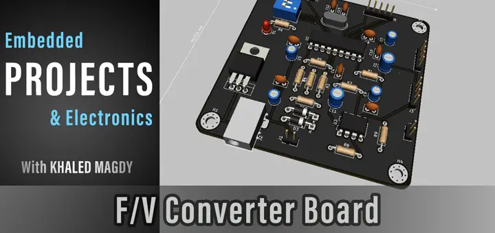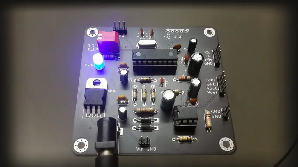
In this project article, I’ll be showing you how to design a very simple F/V converter board from scratch all the way up to fabricating the PCB and doing the final testing. Please, be advised that it’s going to be an educational project as a lot of the design decisions that I’ve made will reflect this as we go through the project steps. I’ll be solving some problems in certain ways that will hopefully teach you something new rather than being “the most efficient” way of doing things.
The project goal is to design an embedded system (hardware/firmware) that takes in a frequency input signal. Maybe from a motor encoder or whatever and measure the frequency then convert it to analog voltage signal at the output. Of course, F/V converter integrated circuits (ICs) and other solutions are viable options indeed. However, for this project, we’ll try to build a customized discrete embedded solution at a very low-cost price point. And hopefully, you’d learn something new down the road.
Without further ado, let’s get started!
| This project is sponsored by JLCPCB. One of the market-leading PCB manufacturing services in the entire world with extremely competitive prices starting from 2$/5boards. And a very high-quality PCB fabrication as we’ll see at the end of this project while testing our board. |
[toc]
System’s Functional Description
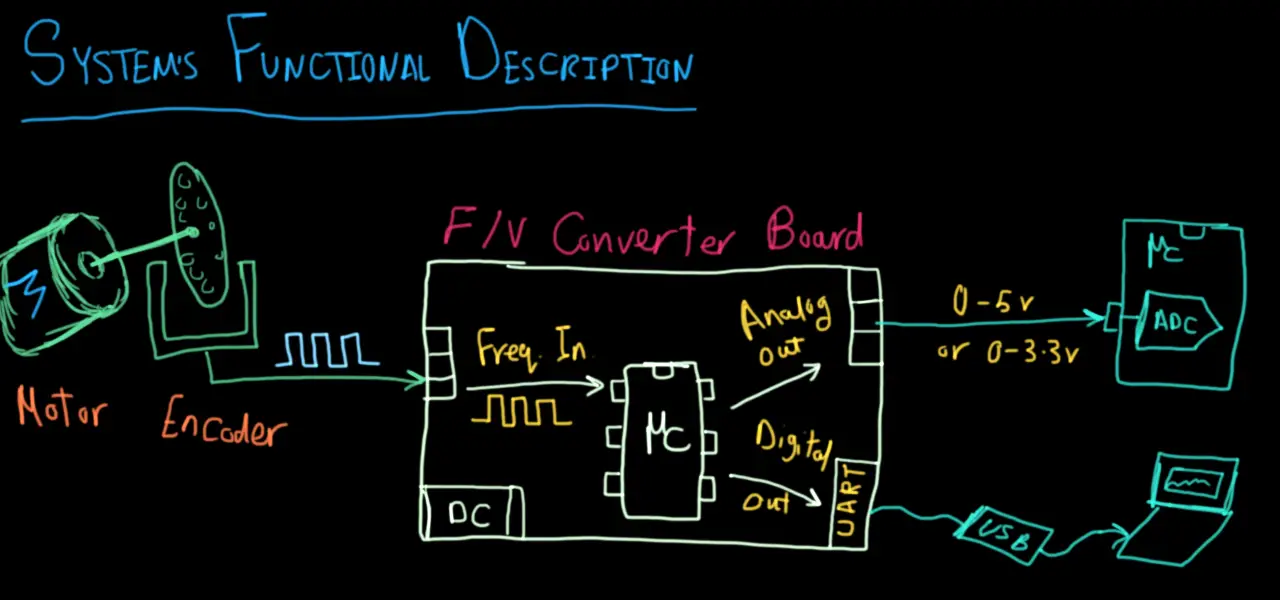
The figure down below shows you the functional description diagram for the system we’re going to design. As you can see, it takes in a frequency input signal from a motor optical encoder sensor, measures the frequency / RPM, and convert it to voltage output at the analog output end. And it also sends out the measured frequency or RPM as a digital UART string message.
The centerpiece on the board is going to be a small 8-bit microcontroller and everything else will be built around that chip to handle all the necessary functionalities as we’ll see in the following design steps.
System Requirements & Design Specs.
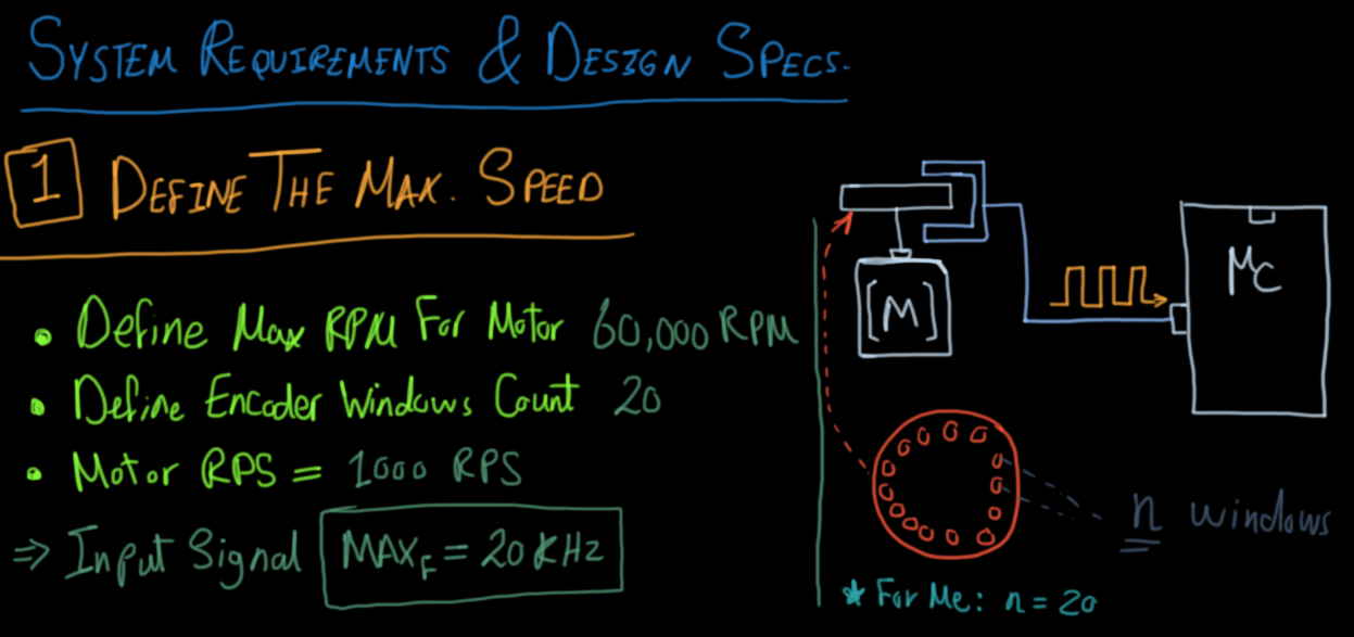
In this section, we’ll be stating the system requirements based on the design specs that we want to achieve at the end of the day. First of which, is the maximum measurable motor speed in RPM. After deciding on the maximum speed range, we can figure out the frequency of the input signal to be measured.
Which depends on the encoder windowed wheel and specifically the number of windows “n”. By having all this information together, we can determine the maximum frequency of the input signal that our microcontroller can expect to read from the encoder sensor.
Defining The Conversion Resolution
The next design specification to be decided is the F/V conversion resolution. What is the minimum motor speed change that induces a change to the output voltage? (in RPM)
Let’s say we want to set the resolution to about 1 RPM. This means that for each RPM of the motor, the system’s output will change by one step.
Then we’ll have also to decide on the output step size which defines the required DAC output resolution consequently. And as you can see in the figure below, if the maximum frequency “at the max RPM” is 20kHz and the minimum “defined by the resolution 1 RPM” is 20Hz, then there are 1000 steps in the entire spectrum.
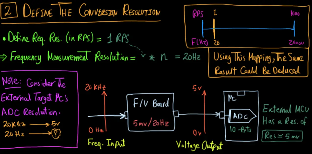
For achieving the analog output functionality, we can use an external DAC chip or even use a microcontroller with a builtin internal DAC module. However, none of those options will be used in this project as we’ll see next.
Design Decisions #1, 2
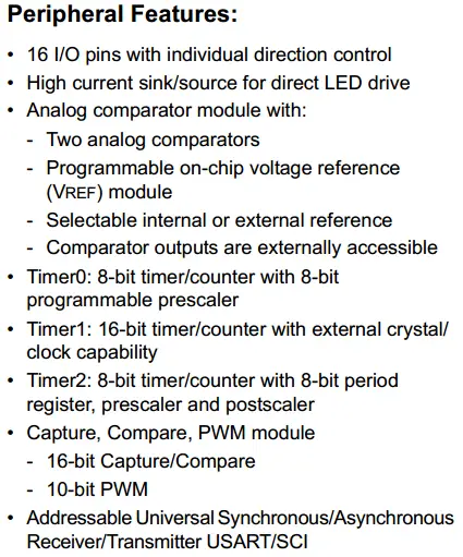
The first two design decisions are to use the 8-bit PIC16F628A microcontroller and use its PWM peripheral with a low-pass filter (LPF) as a DAC for the analog output. And here is a snapshot of the features/peripheral of this small microcontroller chip.

Required PWM Resolution
At this point, we want to find out what is the required PWM resolution in order to achieve the previously determined conversion resolution. In this way, we can properly set up the PWM peripheral and do the math in the application’s code.
It turns out to be 10Bits as you can see from the figure below. Which is fortunately supported by our uC as it has actually 1 PWM output with 10Bits of resolution.

Let’s Wrap Things Up Till Now!
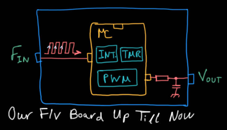
The PCB board we’re going to create has now a microcontroller at the core. Which takes in the input signal from an external encoder sensor or whatever, measure its frequency using the EXT_INT pin and timer module. Then convert the reading to an analog voltage at the output.
The PWM here is used as a DAC to generate analog output voltage after being filtered through an RC low-pass filter (LPF). That’s all about it up till this moment.
LPF Buffered Output
The next challenge is that as you might have known in electronics theory, we just can’t take the output voltage straight out of the LPF capacitor terminal. However, it might seem ok, but it actually isn’t at all!
This type of DAC is typically referred to as “Non-Buffered DAC” which means the voltage output signal is prone to drop if you hook up a reasonably high load at the output. And to protect our system against such a situation, we’ll have to buffer the output voltage to eliminate the possibility of having output voltage fluctuation due to loading effects.
Design Decisions #3
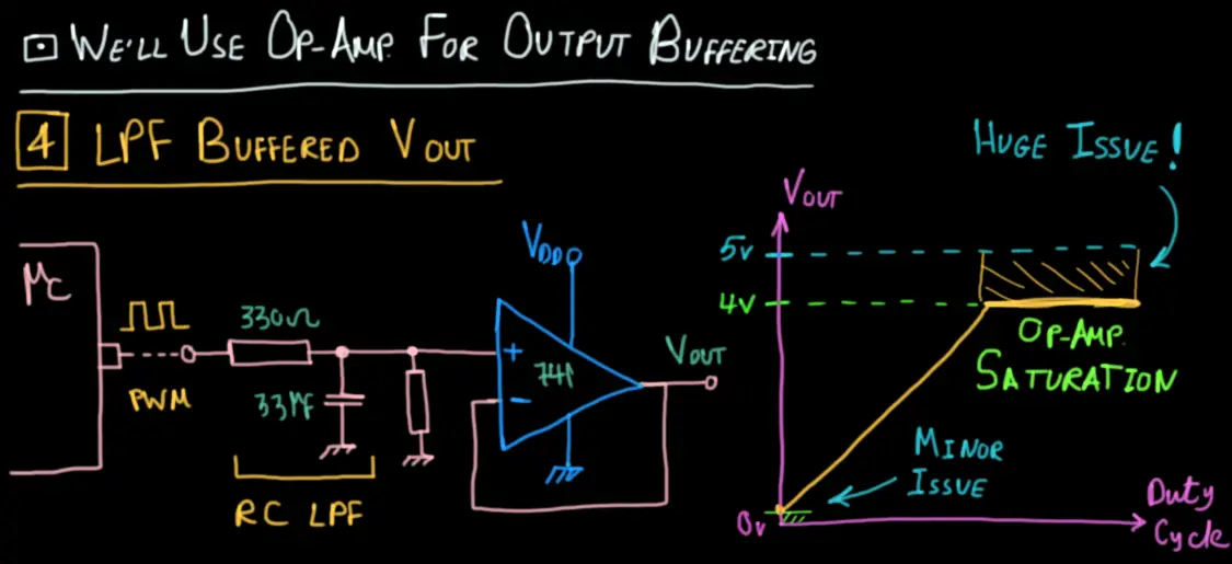
By using an Op-Amp to buffer the PWM-DAC output voltage, we now have solved the signal buffering challenge but 2 issues arise. A major issue: which is op-amp saturation early before the Vcc voltage which is +5v. The op-amp can saturate maybe at +4v which means as the Duty Cycle increases, the output voltage will linearly increase until it hits the saturation point! Very early, unfortunately!
A mitigation for this issue can be using a Rail-To-Rail op-amp which can actually give an output swing from 0 up to +5v easily, hence the name “Rail-To-Rail”. However, it’s a little bit costy which violates the purpose of this system to be a cheap solution. Another solution can be to power up the entire system with +6v or more to work around this issue.
In the next section, we’ll see the design decision and the proposed solution to this issue which may be interesting to you if you didn’t know about it before.
The minor issue in using an op-amp as a buffer is the null offset. Could you notice in the figure above the very tiny voltage offset for the output? That’s what I mean here. This means that at 0% PWM Duty Cycle, the output voltage will not be 0v, instead, it’d be something like 2mv or so.
Good mitigation for this issue can be adding a null-offset resistor according to the op-amp datasheet. However, for the sake of laziness, I’d not bother doing this in my design.
Charge-Pump Output Driver For Op-Amp
Well, do you know that our small uC can output a voltage signal more than +5v in amplitude? Yea! it actually can by using a simple circuitry technique called “Charge-Pump”. It can be made to “double” the output voltage or even more multiples with more modifications.
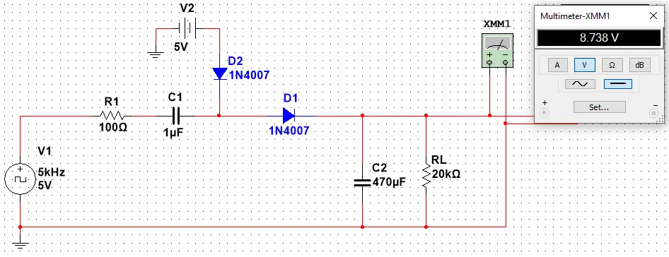
By providing an oscillating clock signal (with a frequency > 1kHz) to this circuitry the charge will keep accumulating on the output capacitor to the point where it reaches (2Vdd-2Vd) which is about (10-1.5 = 8.5v).
And that’s enough for our op-amp! We can pump up the op-amp positive rail up to maybe 8v which is enough to eliminate the early saturation issue without the need to get an expensive op-amp.

You can test this circuitry and play around with the numbers in simulation to validate the concept and you can also search online for more info if you’re interested in this topic. The simulation files will be included in the project downloadable attachments folder at the end of this article.
Note that the output capacitor can be anywhere in the range (10uF to maybe 470uF or more). The larger this output capacitor the lower frequency needed to be feed into the charge-pump. Which is quite good to keep this section of the system in balance.
Here I’m feeding in a 5kHz clock signal which simulates the +5v clock output from the microcontroller. I’ve added a 20k ohm load resistor to simulate the Op-Amp being loaded. And the output voltage is roughly 8.7v as shown on the DMM window.
Oscillating Clock Signal Generation
Now, the question is how can we generate the oscillating clock signal required for the charge-pump? Especially when you know that our uC has only one PWM output pin which has been already reserved for the DAC functionality.
Can we use a timer interrupt to toggle a GPIO pin in order to achieve this required clock output? Well, it can be a solution but even a 1kHz clock would require the CPU to handle 2000 interrupts/sec. This is quite excessive and really bad as we’re doing an interrupt-based frequency measurement work and we want it to be as deterministic as possible.
Another workaround can be to expose the CPU clock signal out to a GPIO pin. What? Yea! it’s possible and a viable option of course. However, the CPU will be running at 20MHz and the output clock signal will be about 5MHz which is too much actually and requires specific routing for this track on the PCB at the end.
The solution for this challenge that I wanted to show you is that you can use the internal comparator module inside the microcontroller as an oscillator. Yea! it can be turned into a relaxation oscillator and give out a TTL clock signal as we’ll see hereafter.
Design Decisions #4
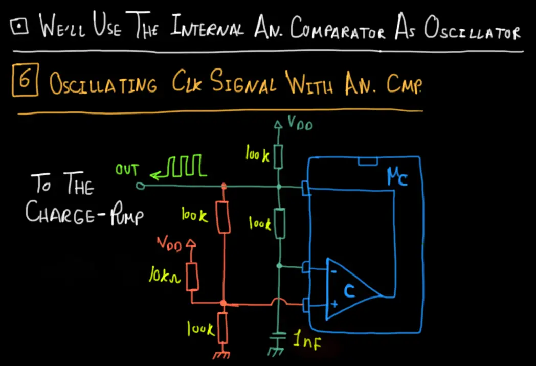
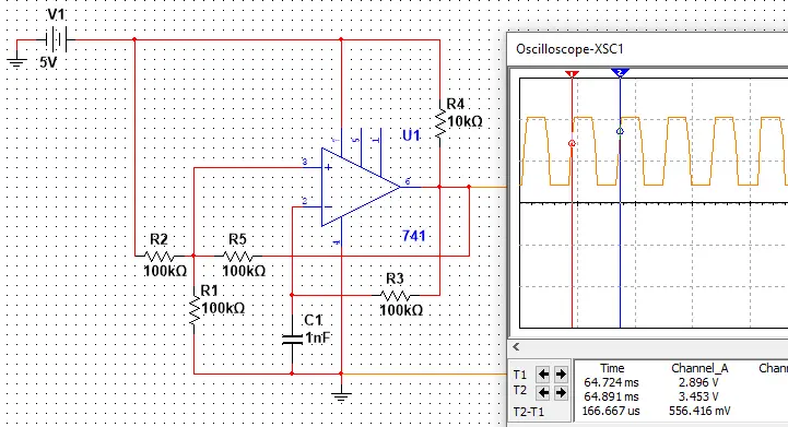
And finally, we can wrap things up and I’d like to declare that no further challenges to be solved in this project anymore. But before proceeding to the next step, let’s run a simulation test for the comparator-based oscillator circuitry and see how it works and how to set up the output frequency by changing the capacitor value or the charging resistor.
Software Layered Architecture
After being done with the top-level design and planning for the project, we can now proceed to the firmware design step. Starting with the software layered architecture overview “Static Design”. In which, we decide on the required software components and the layers in the whole project.
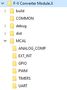
As you can see in the figure below, there are only two layers in this simple architecture. The top “Application Layer” in which we’ll develop the target application. And the MCAL layer (Microcontroller Abstraction Layer) which includes all the hardware peripherals drivers (libraries) which directly interacts with the low-level hardware registers of the machine.
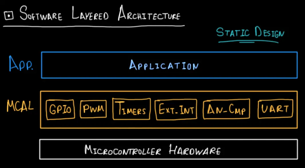
The MCAL layer includes the following drivers for the respective purposes:
- GPIO: for input/output pins used for configuring the board options
- PWM: used as a DAC after being filtered with an LPF
- Timers: used to measure the input signal’s frequency
- EXT_INT: external interrupt for measuring the input signal’s frequency
- AN_CMP: used as an oscillator with a handful of external resistors and capacitor
- UART: used to send out the measurement result as a serial string “digital out”
The Complete Hardware Functional Diagram
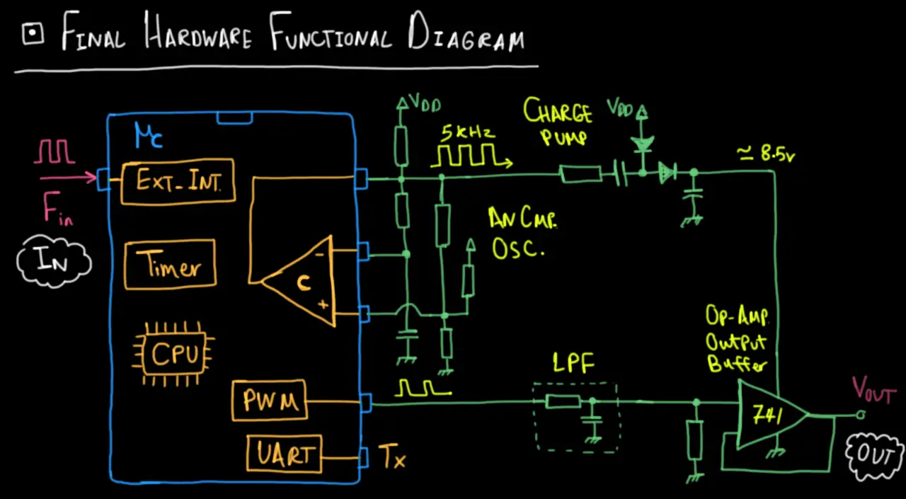
Just before we get into the firmware application code, it’s better to have a look at the big picture of the system. Down below is a functional diagram of the system’s hardware connecting all the pieces together so you can easily see which part does which functionality.
Let me read out aloud what we can see in this diagram. The motor encoder signal (frequency) fires interrupt signals at the rising edges which trigger the timer module to start/stop and measure the period of the signal. And therefore, the frequency is captured.
The analog comparator is set up in independent mode with output pin exposed to A3 pin and the external resistors/capacitor will make it operate as an oscillator with a TTL output that feeds into the charge-pump circuit which in turns provide about 8.5v to the op-amp down below.
The PWM is used as a DAC after getting the PWM signal filtered through the LPF, it gets buffered using the op-amp which is set up in such a way that guarantees a full output voltage swing from 0v up to +5v.
The measured frequency/speed is also sent out through the UART module as a digital output and that’s all.
Firmware Application Code
Now, it’s time to develop the firmware required for this project. And first of all, getting the hardware drivers ready. In the downloadable project files, you’ll find the complete source code for this project so that you can scan through it to see how it’s organized.
And keep in mind that only fundamental functionalities are implemented in code just to run the target application at the end with the least effort possible. I have to disclaim again that all drivers and libraries not generic enough to support any further work beyond the scope of this project.
The application layer has only 1 file which is the main.c file. And the MCAL layer directory has the following sub-directories for the hardware basic drivers. That initializes the different hardware peripherals and run some basic functionalities required by the application layer.
For the application code (main.c), it’s shown down below, and here is a breakout for what’s going on in this application.
The first thing to note, that this system is an interrupt-driven one. Which means the main super loop is empty. Main tasks are handled in the ISR routine as you can see in the attached code.
The other thing to note is that this system keeps switching from one state to another. It’s a simple FSM (Finite-State Machine) with a state variable called Measurement_FSM. The first rising edge interrupt of the input EXT_INT pin drives the system into GOING state which triggers the timer module to start counting the time.
Upon receiving the second rising edge on the EXT_INT pin, the system switches to the DONE state and stops the timer. Then take the measurement convert it to an analog voltage by updating the PWM duty cycle and also send out a UART string with the measured value.
And repeat…
|
1 2 3 4 5 6 7 8 9 10 11 12 13 14 15 16 17 18 19 20 21 22 23 24 25 26 27 28 29 30 31 32 33 34 35 36 37 38 39 40 41 42 43 44 45 46 47 48 49 50 51 52 53 54 55 56 57 58 59 60 61 62 63 64 65 66 67 68 69 70 71 72 73 74 75 76 77 78 79 80 81 82 83 84 85 86 87 88 89 90 91 92 93 94 95 96 97 98 99 100 101 102 103 104 105 106 107 108 109 110 111 112 113 114 115 116 |
/* * File: main.c * Author: Khaled Magdy * * Created on April 18, 2020, 2:42 AM */ #include "COMMON/CONFIG.h" #include "COMMON/STD_TYPES.h" #include "MCAL/PWM/PWM.h" #include "MCAL/EXT_INT/EXT_INT.h" #include "MCAL/ANALOG_COMP/AN_COMP.h" #include "MCAL/TIMERS/TIMERS.h" #include "MCAL/UART/UART.h" #include "MCAL/GPIO/GPIO.h" #include <stdio.h> #define MAX_F 20000 #define MIN_Ticks 250 #define MAX_Ticks 250000 #define OFFSET_CAL 8 #define DONE 1 #define GOING 0 static volatile uint8_t Measurement_FSM = DONE; static volatile uint16_t TMR1_IC = 0; static uint32_t Ticks = 0; static uint16_t F = 0; static uint16_t OUT_DutyCycle = 0; static double T = 0.00; static uint8_t TX_Buffer[10]; void SysInit(void) { GPIO_Init(); AN_COMP1_Init(); PWM1_Init(); INT0_Init(); TMR1_Init(); UART_TX_Init(); } void main(void) { SysInit(); while(1) { } return; } void __interrupt() ISR(void) { if(INTF) { if(Measurement_FSM == DONE) { // Start The Timer Module TMR1ON = 1; // TMR1_IC = 0; Ticks = 0; // Flip The FSM State Variable Measurement_FSM = GOING; } else if(Measurement_FSM == GOING) { // Stop The Timer Module TMR1ON = 0; // Get The Total Timer Ticks Count if(TMR1_IC) { Ticks = (uint32_t)(TMR1 + (TMR1_IC << 16)); } else { Ticks = TMR1; } Ticks -= 6; // Calculate The Signal Frequency F = (uint16_t)(1.0/(((Ticks<<2)/20000000.0))); if(F <= MAX_F+20) { if(V_SEL == V_5) { OUT_DutyCycle = (uint16_t)(F/19.55034); } else if(V_SEL == V_3o3) { OUT_DutyCycle = (uint16_t)(F/29.629); } PWM1_Set_DC(OUT_DutyCycle); if(DO_EN == UART_ENABLED) { sprintf(TX_Buffer, "%d\r\n", F); UART_Write_String(TX_Buffer); } else if (DO_EN == UART_DISABLED) {} } else { } // TMR1 = 0x00; // Flip The FSM State Variable Measurement_FSM = DONE; } INTF = 0; } if(TMR1IF) { TMR1_IC++; TMR1IF = 0; } } |
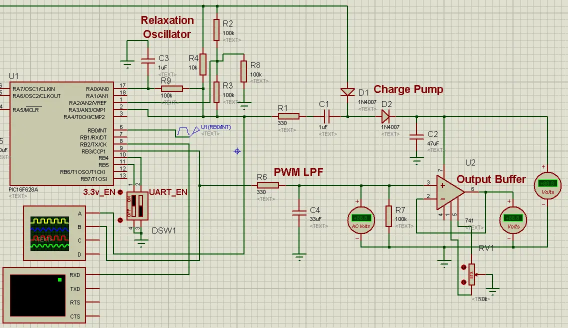
This firmware, partially or fully, can still be simulated on software tools like proteus in order to validate certain functionalities or all of them if it’s possible. I’d advise against this in fact due to the lagging issues that are likely to arise and also numerical convergence in oscillator circuitry simulation which would result in a dead low signal at the output for no reason.
But all In all, you can still run a partial simulation for this project if you’d like to.
Prototyping & Testing
We can now start making our first prototype on a breadboard just to test the hardware and firmware parts of this project. Here is a short demo video for the running test on the breadboard. Just to validate everything before moving on to designing a PCB for the project hardware.
It’s crucial to test and validate every aspect of the system before moving on to making a PCB design. To avoid having to go through a rework revision of the board in the future. In many cases, you’d need to rework the PCB for improvements but having a major issue that prevents it from even working is really disappointing and you’d not like to experience that many times.
Unfortunately, it wasn’t recorded in English! However, you’ll see the board wiring. By testing a 10kHz input signal, the output will be 2.5v exactly. If you still remember the full input frequency range is (0Hz -> 20kHz) and the output will be (0v -> 5v) so the point in the middle of the range checks ok in the first test.
Then, I’ll check a 20kHz input signal, and the output will turn out to be nearly exact 5v which is perfect.
And finally, I’ll set up the Function generator to sweep the frequency from 0Hz up to 20kHz. And our board output voltage will be linear sweep from 0v up to 5v back and forth. This is a linearity check over the entire input range just to validate the system at all possible input frequencies. The output will be a linear triangular wave on the DSO. It might seem discontinuous in time but it’s due to a long time of measurement and DSO data points compression on the screen.
[The Prototyping & Testing Demo Video Starting From 54:42]
Hardware PCB Design
Schematic Design & Capture
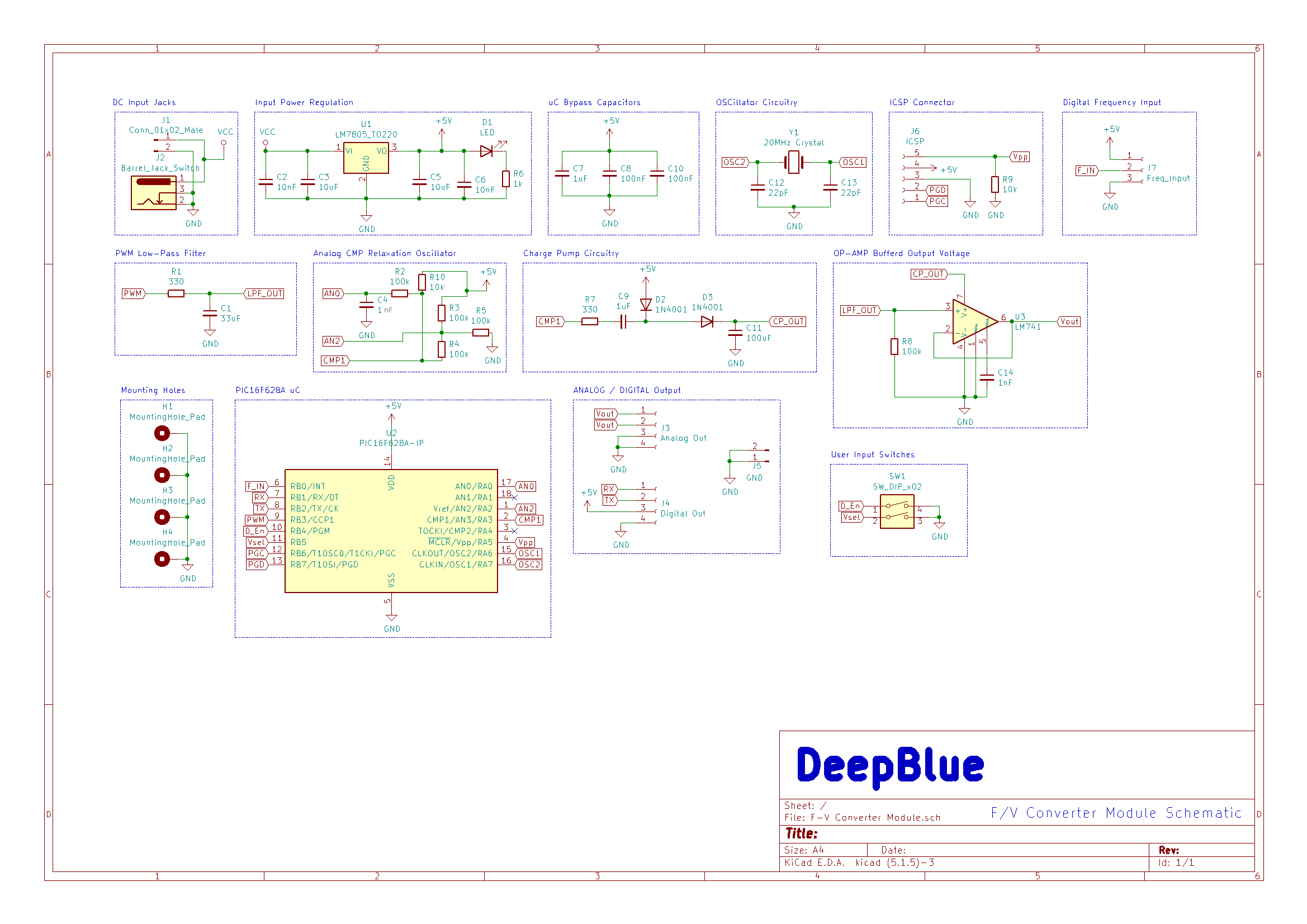
The first step in the PCB design is to finalize the schematic design of the board and then do the schematic capture to the CAD software tool. The PCB design tool that I’ve used for this project was KiCAD. And here is a screenshot of the finalized schematic design for the board.
it’s going to help you so much when it comes to figuring out which part is which while assembling the board. I think I’ve missed generating the BOM file for this board which could serve this purpose a lot better.
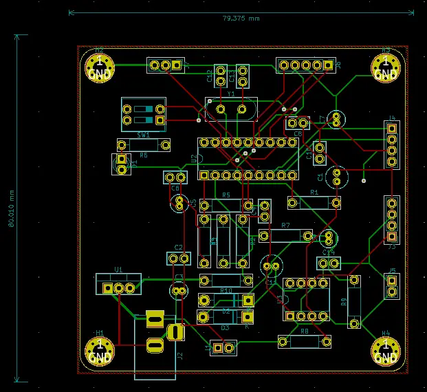
PCB Layout Editing & Routing
Generating Fab.-Ready Output Files (Gerber)
The final step is to generate the fabrication-ready output files (Gerber) to be sent later for manufacturing.
If you’re interested in PCB design with KiCAD, you can check my course on Udemy! it’s on SALE and you can get it for maybe 10$ or something. And in case you can’t enroll for whatever reason, just join my email list to get a 100% FREE coupon whenever I’ve free coupons, I’ll send to all my list subscribers. So it can be something to consider.
PCB Fabrication & Assembly
I’ve chosen to go with JLCPCB when I first designed this board and still highly recommend this service to anyone. It’s by far the best I’ve ever used in terms of quality, speed, and low cost. Its competitive price point makes it a market-leading company in this area. You can use this promo code “JLC-REBE” which is permanent (never expires) to get 2$ offer fabrication for your 5 boards.
Step1: Go to JLCPCB.com & Click on “Quote Now”

Step2: Upload the Gerber files to JLCPCB

Step3: Choose the board color, fabrication options, and quantity
Step4: Place the order, Write Your Shipping Address, and Pay the due amount
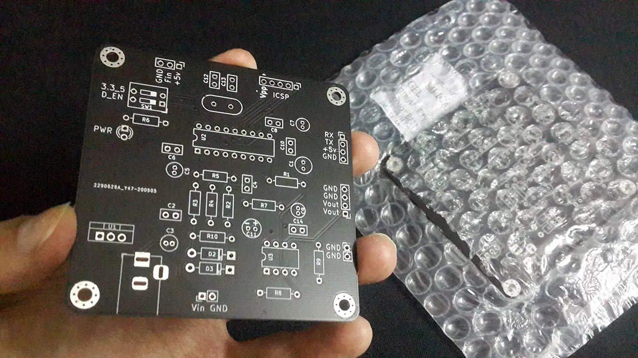
Now, you’ll have to wait the turnaround time for JLCPCB fabrication which can be 24hours for standard options. And maybe up to 3 days in case you choose fancy options for your board like the matte black color finish which I absolutely love for all of my boards <3
Here is how it looked like when I’ve received the boards
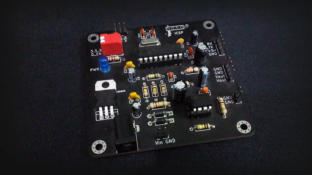
After soldering & assembling the PCB
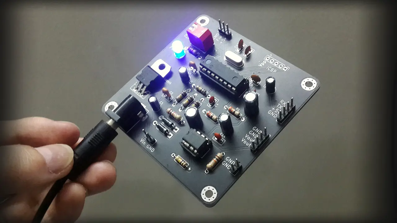
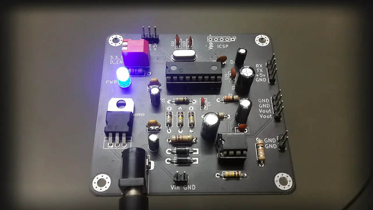
Power Up For The First Time!
Final Hardware Testing
After flashing the firmware to the microcontroller and powering up the board through the DC jack, it’s time to take some measurements and do some tests. First of which is to make sure that the analog comparator module is up and running as an oscillator.
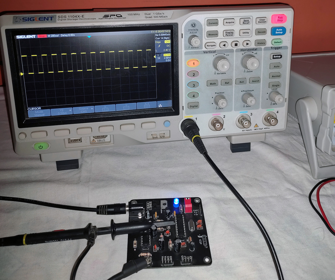
Here I’m hooking my DSO probe to the output pin of the comparator oscillator (A3) and the signal looks perfect! The frequency is about 5kHz and it can be changed by changing the value of the (C4) capacitor and the charging resistor in the oscillator circuitry. But 5kHz is very enough to feed in the charge-pump circuit at the end.
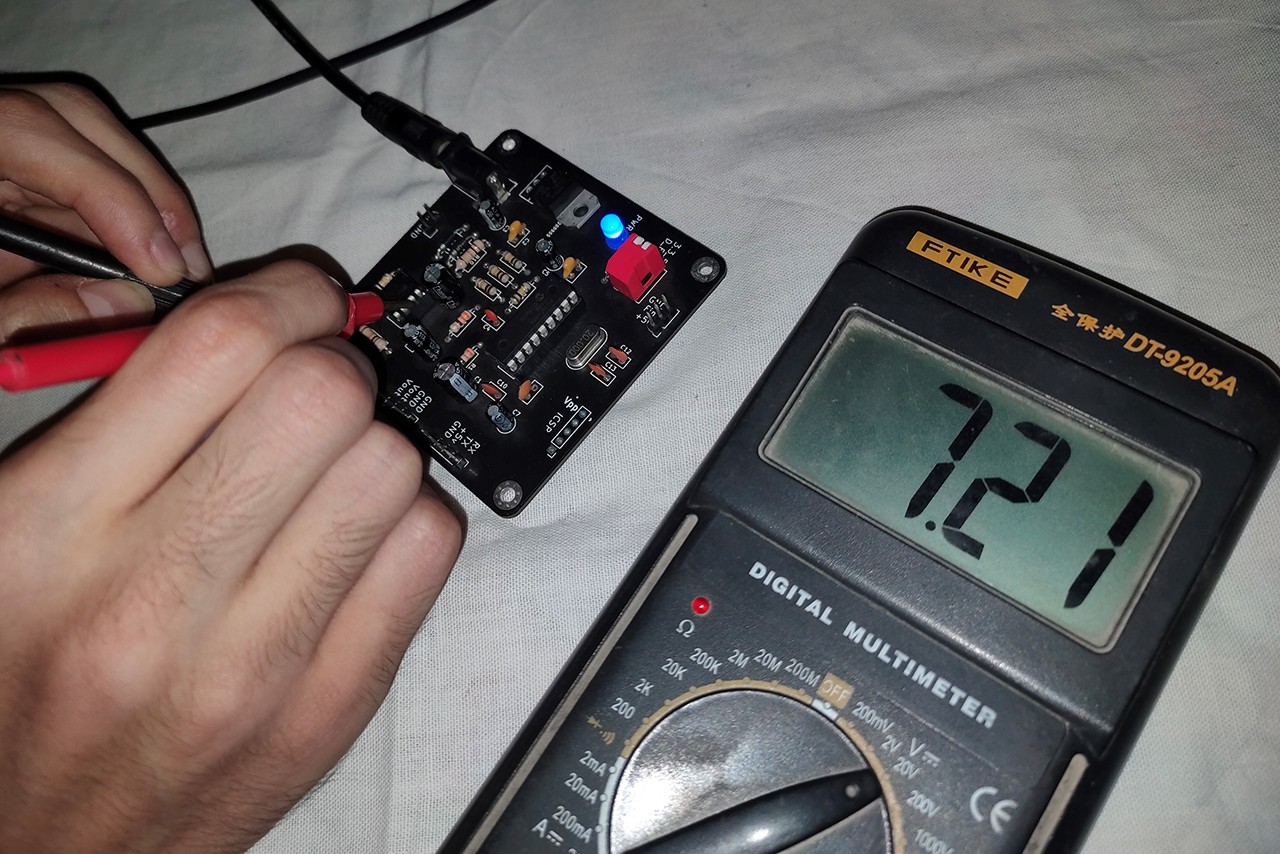
Now, we need to have a look at the charge-pump circuit’s output voltage. The oscillator is working ok and the charge-pump should also, hopefully, be the same. I’ll read the voltage at the +Vcc pin on the op-amp using the DMM. And it happens to be 7.2v which is very good enough.
Please, remember that the 8.5v was a rough estimation dependent on an arbitrarily chosen load value in the simulation we did (the 20k ohm resistor), and in real-world it turned out to be loaded a little bit more which causes the drop-down to 7.2v. And it’s still more than enough to give our op-amp the headroom to swing up to +5v easily.
I’ll try to shoot a short demo video for measurement testing or at least upload some photos. I did actually test the boards for this project back in the days when it was complete and missed to document that work for some reason.
Concluding Remarks
✓ Download The Project Attachments Folder
✓ As I’ve stated at the beginning of this project. It’s an educational project to help you learn about a couple of topics in an engaging and experimental way. Which can be seen as an over-engineered F/V converter board! Yea it can be made easier than this of course but in the name of science, everything is allowed!
✓ If you’ve got any further questions or need help in a project you can drop me a comment down below or contact me via emails. I’ll do my best to help as much as I can.
✓ If you feel like really into PCB design and making your own boards. Please, check out my course on PCB Design For Embedded Systems. It’s growing in popularity and has been on the “Highest Rated” on Udemy since published. So, check it out!
✓ In case you find this website helpful, please consider supporting my work on patreon. I’d really like to grow that campaign in order to be able to take down a lot of the random google ads scattered all over my website. I don’t really like it as much as most of the readers. But with +50k readers/month there are only 3 partons, it’s quite difficult maybe.
