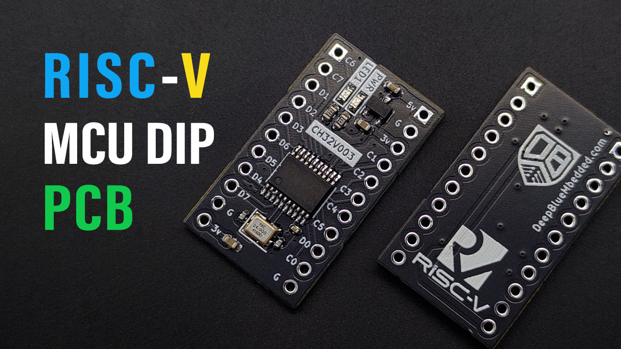
In this article, I’ll show you the CH32V003 schematic & PCB design steps, explain some of the design aspects, how to prepare the files needed for manufacturing, and how to place the PCB SMT order at JLCPCB who are kindly sponsoring this project as well.
This is a custom development board built around the CH32V003 which is known on the internet as the “10 cents RISC-V microcontroller” from WCH. This project can serve as a baseline for anyone willing to create his own RISC-V MCU dev board based on the CH32V003 microcontroller.
You may also need to check out my other CH32V003 dev board PCB design project linked below.
This is another project around the CH32V003 RISC-V microcontroller. You may want to have a look at its schematic design, firmware test examples, etc.
This Project is Sponsored By JLCPCB
Table of Contents
- CH32V003 Overview & Datasheet
- CH32V003 Dev Board Schematic Design
- Placing PCBA Order @ JLCPCB
- CH32V003 LED Blinking GPIO Example Test
- CH32V003 PWM Example Test
- CH32V003 UART Example
- CH32V003 ADC-PWM LED Dimmer Example
- Concluding Remarks
- CH32V003 Schematic + PCB Design Project Video
CH32V003 Overview & Datasheet
The CH32V003 is based on the QingKe RISC-V2A core design of an industrial-grade general-purpose microcontroller, that supports 48MHz system main frequency, ADC, DMA, and a handful of other peripherals. Here is a block diagram of the microcontroller’s top-level architecture.

CH32V003 Variants & IC Packages

CH32V003 Datasheet & Reference Manual
CH32V003 Dev Board Schematic Design
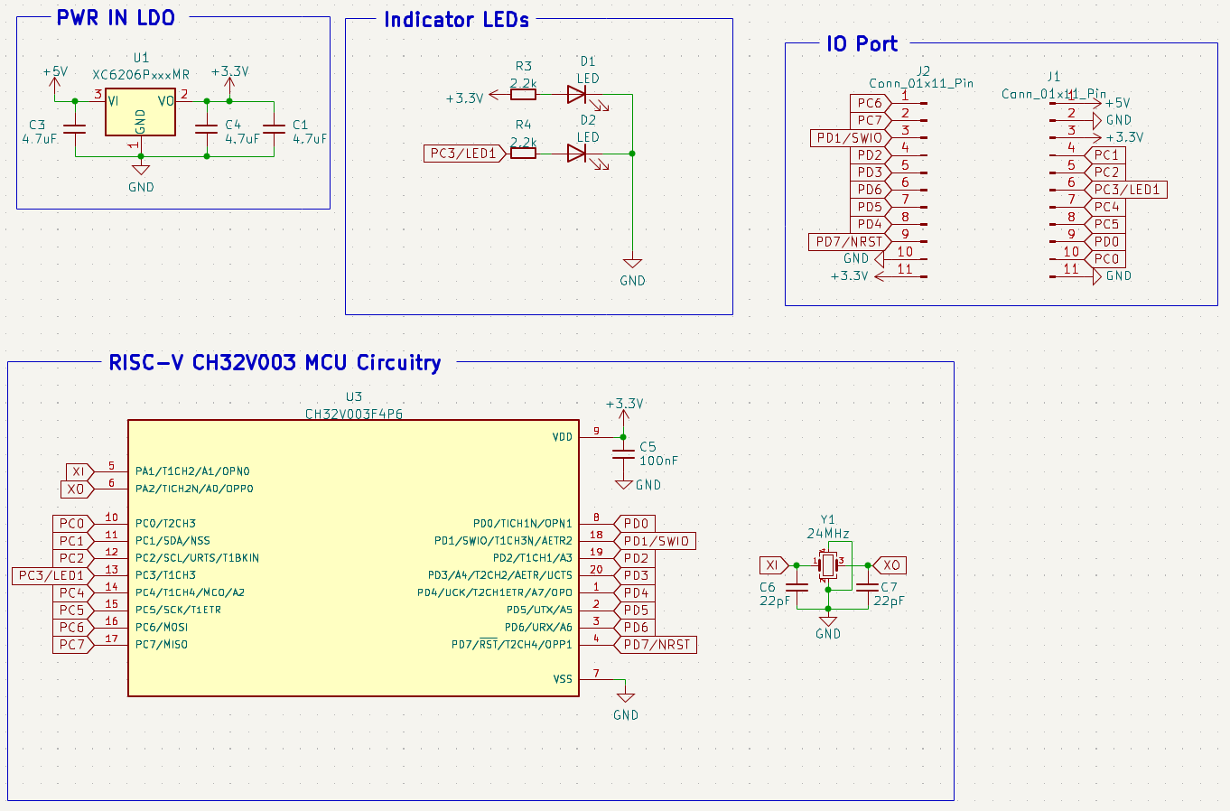
This is the schematic design that I came up with for this CH32V003 development board project.
1. DC PWR In + LDO
The +5v input pin is regulated down to 3.3v using an LDO. The 3.3v is then used to power up the CH32V003 microcontroller.
However, if you’d like to, the CH32V003 can and will operate at a regulated +5v input power source. The (digital peripherals, IO pins, ADC, and analog circuits) will adjust and work fine with that voltage. All IOs are 5v-tolerant in this microcontroller.
2. CH32V003 MCU Circuitry
The CH32V003 microcontroller requires a 3.3v input voltage @ Vdd pin, a 100nF decoupling capacitor, and a 24MHz crystal oscillator.
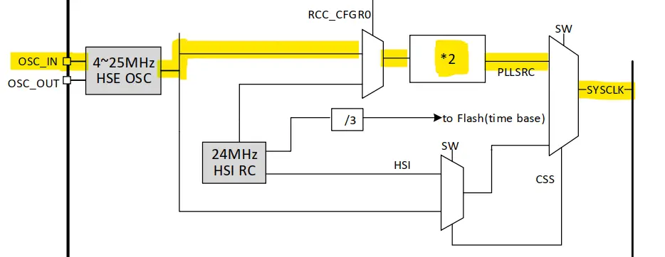
You can use any crystal oscillator frequency you want, however, it’s necessary to use a 24MHz if you want to run the MCU at its maximum speed @48MHz. This is because the internal PLL is not arbitrarily programmable as in STM32 microcontrollers for example. The internal PLL just multiplies the input clock frequency by 2 and that’s it.
I’ve also added an NRST button to reset the microcontroller when needed.
3. IO Ports + LEDs
Just pin-out all the IO pins to two headers depending on your desired board shape and layout.
I’ve added a power indicator LED + 1x user-programmable LED. I wanted the LED to be PWM-controlled, so I made sure it was hooked to a TxCHx pin on the CH32V003 microcontroller.
The CH32V003 supports a serial wire debug using only one line if you’re going to use the WCH-Link debugger as the one shown below.
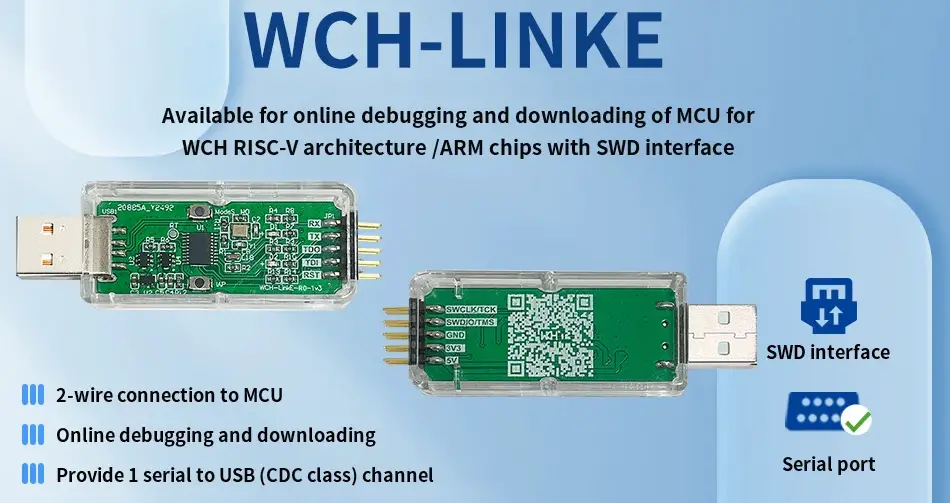
This debugger has an internal USB-UART bridge that you can use instead of adding a dedicated chip for that purpose. We’ll use this USB-UART for testing our project today.
Placing PCBA Order @ JLCPCB
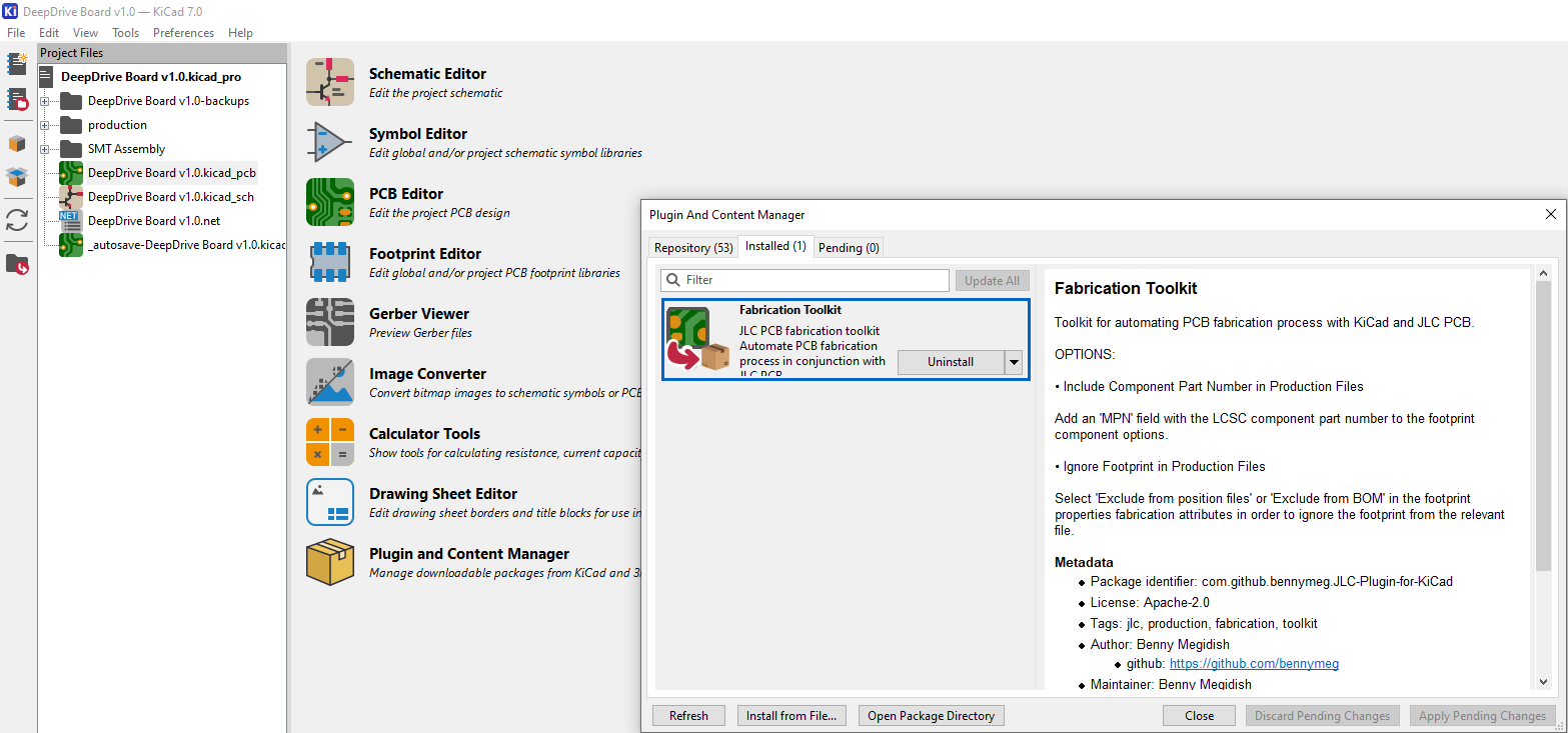
Finally, we’re ready to generate the fabrication files and send them to JLCPCB for PCB fabrication and assembly. For this task, I use the KiCAD plugin named “Fabrication Toolkit”. With just one button click, you’ll have all manufacturing output files ready in a new folder that’s automatically created for you by the plugin toolkit.
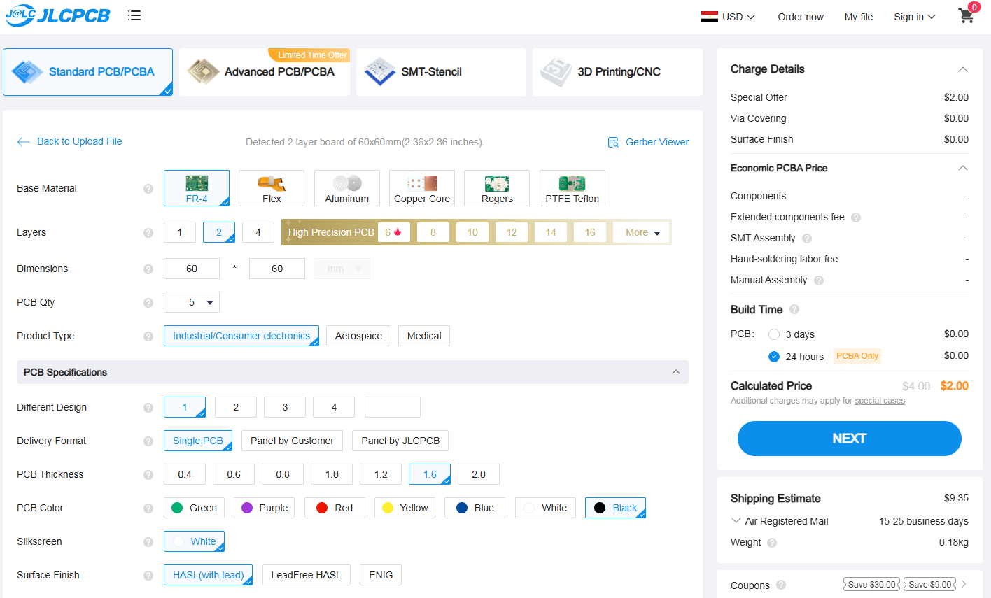
1. Upload Your Gerber File & Check PCB Fab. Options
The next step is to upload your PCB Gerber files and modify the PCB fabrication options as needed in your project. Just keep an eye on the price because some options are not considered as a standard fabrication process, which will end up costing you a bit more and take a bit more time to get fabricated.
Even if you’re 100% sure that your design and fabrication files are flawless, the online system at JLCPCB, or any other fab house, can still pick up the wrong components orientation or placement. Always double-check the PCB component placement after uploading your files.
2. Upload BOM & CPL Files
The next step is to upload your design’s BOM file and the components positions file (CPL) to JLCPCB and let it check the files and report the stock status and total number of components to be assembled, their cost, and so on.

Check everything and make sure the components are selected correctly from the JLCPCB SMT library. And also double-check the component placements on the next page and correct any wrong rotations in the CPL file. There is a mismatch between the KiCAD output position file & JLCPCB’s system, so it does pick up wrong orientations for some ICs, diodes, etc. Always double-check everything before placing the order.
3. Pay To Place Your Order
The last step to place your order is to pay for the invoice and you can apply any valid discount coupon at this step to reduce the cost.
4. Wait For Delivery & Prepare For Testing!
You should expect to receive your board within 4 days to 1 week depending on where you live.
Here is what the boards look like after unboxing the JLCPCB package. We’ll solder some pin headers to one of these PCB boards, put it onto a breadboard, and we’re ready for testing.

CH32V003 LED Blinking GPIO Example Test
This is the first test example project in which we’ll blink the onboard LED.
Open the MounRiver IDE, create a new project using NoOS Tempelate, and copy the example test code below.
CH32V003 LED Blinking GPIO Example Code
The Application Code For This Example (main.c)
/*
 * LAB Name: CH32V003 GPIO Test
 * Author: Khaled Magdy
 * For More Info Visit: www.DeepBlueMbedded.com
*/
#include "debug.h"

void LEDs_GPIO_Init(void);

int main(void)
{
    NVIC_PriorityGroupConfig(NVIC_PriorityGroup_1);
    SystemCoreClockUpdate();
    Delay_Init();
    LEDs_GPIO_Init();

    while(1)
    {
        GPIO_SetBits(GPIOC, GPIO_Pin_3);
        Delay_Ms(100);
        GPIO_ResetBits(GPIOC, GPIO_Pin_3);
        Delay_Ms(100);
    }
}

void LEDs_GPIO_Init(void)
{
    GPIO_InitTypeDef GPIO_InitStructure={0};
    RCC_APB2PeriphClockCmd(RCC_APB2Periph_GPIOC, ENABLE );
    // C3 Pin
    GPIO_InitStructure.GPIO_Pin = GPIO_Pin_3;
    GPIO_InitStructure.GPIO_Mode = GPIO_Mode_Out_PP;
    GPIO_InitStructure.GPIO_Speed = GPIO_Speed_30MHz;
    GPIO_Init( GPIOC, &GPIO_InitStructure );
}
Compile & Flash the firmware to the board using the WCH-Link debugger.
CH32V003 LED Blinking Test Result
CH32V003 PWM Example Test
In this test project, we’ll dim the onboard LED using PWM output (TIMER1-CH3).
Open the MounRiver IDE, create a new project using NoOS Tempelate, and copy the example test code below.
CH32V003 PWM Example Code
The Application Code For This Example (main.c)
/*
 * LAB Name: CH32V003 PWM  Test
 * Author: Khaled Magdy
 * For More Info Visit: www.DeepBlueMbedded.com
*/
#include "debug.h"

uint16_t Duty = 0;
int Step = 1;
void TIM1_PWM3_Init(u16, u16, u16);

int main(void)
{
    NVIC_PriorityGroupConfig(NVIC_PriorityGroup_1);
    SystemCoreClockUpdate();
    Delay_Init();
    //LED_GPIO_Init();
    TIM1_PWM3_Init(1024, 0, 0); // TIMER1_CH3

    while(1)
    {
        // Update PWM1-CH3
        TIM1->CH3CVR = Duty;
        Duty += Step;
        // Reverse direction when reaching max or min brightness
        if (Duty == 1024 || Duty == 0) {
            Step = -1*Step;
        }
        Delay_Ms(1);
    }
}

void TIM1_PWM3_Init(u16 arr, u16 psc, u16 ccp)
{
    GPIO_InitTypeDef GPIO_InitStructure={0};
    TIM_OCInitTypeDef TIM_OCInitStructure={0};
    TIM_TimeBaseInitTypeDef TIM_TimeBaseInitStructure={0};
    RCC_APB2PeriphClockCmd( RCC_APB2Periph_GPIOC | RCC_APB2Periph_TIM1, ENABLE );

    // C3 Pin
    GPIO_InitStructure.GPIO_Pin = GPIO_Pin_3;
    GPIO_InitStructure.GPIO_Mode = GPIO_Mode_AF_PP;
    GPIO_InitStructure.GPIO_Speed = GPIO_Speed_30MHz;
    GPIO_Init( GPIOC, &GPIO_InitStructure );

    TIM_TimeBaseInitStructure.TIM_Period = arr;
    TIM_TimeBaseInitStructure.TIM_Prescaler = psc;
    TIM_TimeBaseInitStructure.TIM_ClockDivision = TIM_CKD_DIV1;
    TIM_TimeBaseInitStructure.TIM_CounterMode = TIM_CounterMode_Up;
    TIM_TimeBaseInit( TIM1, &TIM_TimeBaseInitStructure);

    TIM_OCInitStructure.TIM_OCMode = TIM_OCMode_PWM2;
    TIM_OCInitStructure.TIM_OutputState = TIM_OutputState_Enable;
    TIM_OCInitStructure.TIM_Pulse = ccp;
    TIM_OCInitStructure.TIM_OCPolarity = TIM_OCPolarity_High;
    TIM_OC3Init( TIM1, &TIM_OCInitStructure );

    TIM_CtrlPWMOutputs(TIM1, ENABLE );
    TIM_OC3PreloadConfig( TIM1, TIM_OCPreload_Enable );
    TIM_ARRPreloadConfig( TIM1, ENABLE );
    TIM_Cmd( TIM1, ENABLE );
}
Compile & Flash the firmware to the board using the WCH-Link debugger.
CH32V003 PWM LED Dimmer Test Result
CH32V003 UART Example
CH32V003 UART (printf) Example Code
/*
 * LAB Name: CH32V003 UART TX (printf)  Test
 * Author: Khaled Magdy
 * For More Info Visit: www.DeepBlueMbedded.com
*/
#include "debug.h"

uint8_t C = 0;

void UART1_Init(void);

int main(void)
{
    NVIC_PriorityGroupConfig(NVIC_PriorityGroup_1);
    SystemCoreClockUpdate();
    Delay_Init();
    USART_Printf_Init(115200);
    //UART1_Init();
    printf("SystemClk:%d\r\n",SystemCoreClock);
    printf( "ChipID:%08x\r\n", DBGMCU_GetCHIPID() );

    while(1)
    {
        printf("Hello World, Counter = %d\r\n", C);
        C++;
        Delay_Ms(100);
    }
}

void UART1_Init(void)
{
    GPIO_InitTypeDef  GPIO_InitStructure = {0};
    USART_InitTypeDef USART_InitStructure = {0};

    RCC_APB2PeriphClockCmd(RCC_APB2Periph_GPIOD | RCC_APB2Periph_USART1, ENABLE);

    /* USART1 TX-->D.5 */
    GPIO_InitStructure.GPIO_Pin = GPIO_Pin_5;
    GPIO_InitStructure.GPIO_Speed = GPIO_Speed_30MHz;
    GPIO_InitStructure.GPIO_Mode = GPIO_Mode_AF_PP;
    GPIO_Init(GPIOD, &GPIO_InitStructure);
    /* USART1 CFG */
    USART_InitStructure.USART_BaudRate = 115200;
    USART_InitStructure.USART_WordLength = USART_WordLength_8b;
    USART_InitStructure.USART_StopBits = USART_StopBits_1;
    USART_InitStructure.USART_Parity = USART_Parity_No;
    USART_InitStructure.USART_HardwareFlowControl = USART_HardwareFlowControl_None;
    USART_InitStructure.USART_Mode = USART_Mode_Tx;

    USART_Init(USART1, &USART_InitStructure);
    USART_Cmd(USART1, ENABLE);
}
CH32V003 UART (Printf) Test Result

CH32V003 ADC-PWM LED Dimmer Example
CH32V003 ADC LED Dimmer Example Code
/*
 * LAB Name: CH32V003 [ADC (SingleChannel-SingleConv) + PWM] LED Dimmer Example
 * Author: Khaled Magdy
 * For More Info Visit: www.DeepBlueMbedded.com
*/
#include "debug.h"

#define POT_ADC_CH  ADC_Channel_2

void TIM1_PWM3_Init(u16, u16, u16);
void ADC_SingleCH_SingleConv_Init(void);
uint16_t Pot_ADC_Read(void);

int main(void)
{
    NVIC_PriorityGroupConfig(NVIC_PriorityGroup_1);
    SystemCoreClockUpdate();
    Delay_Init();
    TIM1_PWM3_Init(1023, 0, 0); // TIMER1_CH3
    ADC_SingleCH_SingleConv_Init();

    while(1)
    {
        TIM1->CH3CVR = Pot_ADC_Read();
        Delay_Ms(1);
    }
}

void ADC_SingleCH_SingleConv_Init(void)
{
    // Enable the ADC clock
    RCC_APB2PeriphClockCmd(RCC_APB2Periph_ADC1 | RCC_APB2Periph_GPIOC, ENABLE);
    // Configure the ADC pin [ ADC1-CH2 (AIN2) -> PC4 ]
    GPIO_InitTypeDef GPIO_InitStructure;
    GPIO_InitStructure.GPIO_Pin = GPIO_Pin_4;
    GPIO_InitStructure.GPIO_Mode = GPIO_Mode_AIN;
    GPIO_Init(GPIOC, &GPIO_InitStructure);
    // ADC Configuration
    ADC_InitTypeDef ADC_InitStructure;
    ADC_InitStructure.ADC_Mode = ADC_Mode_Independent;
    ADC_InitStructure.ADC_ScanConvMode = DISABLE;
    ADC_InitStructure.ADC_ContinuousConvMode = DISABLE;
    ADC_InitStructure.ADC_ExternalTrigConv = ADC_ExternalTrigConv_None;
    ADC_InitStructure.ADC_DataAlign = ADC_DataAlign_Right;
    ADC_InitStructure.ADC_NbrOfChannel = 1;
    ADC_Init(ADC1, &ADC_InitStructure);
    // Enable ADC
    ADC_Cmd(ADC1, ENABLE);
    // Calibrate ADC
    ADC_Calibration_Vol(ADC1, ADC_CALVOL_50PERCENT);
    ADC_ResetCalibration(ADC1);
    while (ADC_GetResetCalibrationStatus(ADC1));
    ADC_StartCalibration(ADC1);
    while (ADC_GetCalibrationStatus(ADC1));
}

uint16_t Pot_ADC_Read(void)
{
    // Configure the ADC channel
    ADC_RegularChannelConfig(ADC1, POT_ADC_CH, 1, ADC_SampleTime_3Cycles);
    // Start the conversion
    ADC_SoftwareStartConvCmd(ADC1, ENABLE);
    // Wait for conversion completion
    while (!ADC_GetFlagStatus(ADC1, ADC_FLAG_EOC));
    // Get the result
    return ADC_GetConversionValue(ADC1);
}

void TIM1_PWM3_Init(u16 arr, u16 psc, u16 ccp)
{
    GPIO_InitTypeDef GPIO_InitStructure={0};
    TIM_OCInitTypeDef TIM_OCInitStructure={0};
    TIM_TimeBaseInitTypeDef TIM_TimeBaseInitStructure={0};
    RCC_APB2PeriphClockCmd( RCC_APB2Periph_GPIOC | RCC_APB2Periph_TIM1, ENABLE );

    // C3 Pin
    GPIO_InitStructure.GPIO_Pin = GPIO_Pin_3;
    GPIO_InitStructure.GPIO_Mode = GPIO_Mode_AF_PP;
    GPIO_InitStructure.GPIO_Speed = GPIO_Speed_30MHz;
    GPIO_Init( GPIOC, &GPIO_InitStructure );

    TIM_TimeBaseInitStructure.TIM_Period = arr;
    TIM_TimeBaseInitStructure.TIM_Prescaler = psc;
    TIM_TimeBaseInitStructure.TIM_ClockDivision = TIM_CKD_DIV1;
    TIM_TimeBaseInitStructure.TIM_CounterMode = TIM_CounterMode_Up;
    TIM_TimeBaseInit( TIM1, &TIM_TimeBaseInitStructure);

    TIM_OCInitStructure.TIM_OCMode = TIM_OCMode_PWM2;
    TIM_OCInitStructure.TIM_OutputState = TIM_OutputState_Enable;
    TIM_OCInitStructure.TIM_Pulse = ccp;
    TIM_OCInitStructure.TIM_OCPolarity = TIM_OCPolarity_High;
    TIM_OC3Init( TIM1, &TIM_OCInitStructure );

    TIM_CtrlPWMOutputs(TIM1, ENABLE );
    TIM_OC3PreloadConfig( TIM1, TIM_OCPreload_Enable );
    TIM_ARRPreloadConfig( TIM1, ENABLE );
    TIM_Cmd( TIM1, ENABLE );
}
CH32V003 ADC LED Dimmer Test Result
Concluding Remarks
By the end of this, you should have learned how to create your custom CH32V003 dev board or incorporate this microcontroller in your next project if needed. There are lots of firmware examples online from WCH or community-contributed repos that you can reference to accelerate prototyping your project ideas.
MCU Reset Button
You can easily add a manual MCU reset button externally on the breadboard as shown below.

More CH32V003 Firmware Examples
There are lots of firmware examples by WCH for the CH32V003 microcontroller that you can reference here in the link below.
There is also a GitHub repo with so many examples and useful stuff that was recommended to me by Charles, CNLohr (who’s got an excellent YT channel, BTW).
CNLohr CH32V003Fun Github Repo
CH32V003 Schematic + PCB Design Project Video
Here is the video for this project on YouTube if you’d like to get more in-depth information and explanation of the design of this CH32V003 PCB project.
