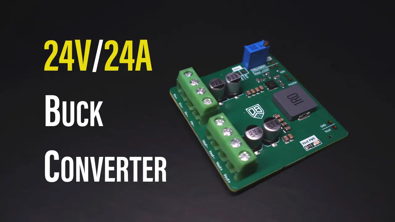
In this article, I’ll show you a DC/DC buck converter PCB project around the SiC431 step-down converter rated for up to 24V and 24A continuous current. We’ll explore the features of this chip, how to design a custom DC/DC buck converter PCB around SiC431, prepare the files needed for manufacturing, and how to place the PCB SMT order at JLCPCB, who are kindly sponsoring this project.
This is a custom DC/DC buck converter evaluation board around Vishay’s SiC431. This project can serve as a baseline for anyone willing to create their own custom board based on the SiC431 step-down buck converter.
This Project is Sponsored By JLCPCB
Table of Contents
- DC/DC Buck Converter Design Overview
- Vishay’s SiC431 24V/24A MicroBuck
- DC/DC Buck Converter Schematic Design
- Placing PCBA Order @ JLCPCB
- 12V To 5V Step-Down Buck Converter Measurements
- 12V To 3.3V Step-Down Buck Converter Measurements
- 24V To 12V Step-Down Buck Converter Measurements
- 24V To 10V @ 20A Step-Down Buck Converter Measurements
- Wrap Up
- [YouTube Video] 24V/24A DC/DC Buck Converter PCB Design Project
DC/DC Buck Converter Design Overview
This DC/DC buck converter project is based on Vishay’s SiC431 MicroBuck chip with a typical application schematic design built on a 6-layer PCB to evaluate the chip’s performance over its entire operating range (up to 24V / 24A).
In this project’s article, we’ll discuss the features/capabilities of the SiC431 chip and how to design a custom PCB project around this chip, and also discuss the potential applications for this DC/DC step-down converter.
Vishay’s SiC431 24V/24A MicroBuck
The SiC431 is a synchronous buck regulator with integrated high-side and low-side power MOSFETs. It only requires an output inductor, a few passives, input/output capacitors, and that’s it. So it’s a very cost-effective solution with minimal BOM requirements + being a 1.2$ chip makes it an even more eye-catching solution.
")
SiC431 Power Stage
The SiC431’s power stage has integrated high-side and low-side power MOSFETs with extremely low RDSon (2mΩ, 6mΩ; optimized for performance, 97% peak efficiency). Its power stage is capable of supplying 24A continuous current at up to 1MHz switching frequency.
This regulator produces an adjustable output voltage down to 0.6V from 3V to 24V input rail to accommodate a variety of applications, including computing, consumer electronics, telecom, and industrial.
SiC431 Safety Features
The regulator integrates a full protection feature set, including:
- Output over-voltage protection (OVP)
- Output under-voltage protection (UVP)
- Cycle-by-cycle over-current protection (OCP)
- Short-circuit protection (SCP)
- Thermal shutdown (OTP)
- Under-voltage lock out (UVLO) + Auto Retry
- User programmable soft-start
DC/DC Buck Converter Schematic Design
For this project, I’ve mainly used the typical application schematic diagram found in the datasheet of the SiC431. Then, I did also check Vishay’s PowerCAD online schematic configurator & generator to check out various operating points, configurations, power simulations, efficiencies, etc.
1. SiC431 Typical Application Schematic
Here is a typical application schematic diagram directly from the SiC431’s datasheet.
")
2. Vishay’s PowerCAD SiC431 Schematic Generator
This is Vishay’s PowerCAD Tool that you can use to set up a custom configuration for your DC/DC Buck converter system, and it’ll generate the schematic diagram for you according to your specific settings. And it’ll also allow you to run simulations, check out output power/efficiency, and many other cool features.
 PowerCAD")
3. My Custom Modifications
For my DC/DC buck converter project, I’ve replaced the feedback top resistor (RFB1) with a 500k trimmer potentiometer to have an adjustable output voltage, but you can of course run it at (single or multiple) fixed output voltage instead.
I made an additional input path to “steer” the buck converter’s output digitally with an external microcontroller in addition to a current DAC. This is risky business that I don’t recommend doing + it introduces some noise and makes your feedback setup less than ideal, to say the least.
Placing PCBA Order @ JLCPCB
Finally, we’re ready to generate the fabrication files and send them to JLCPCB for PCB fabrication and assembly. For this task, I use the KiCAD plugin named “Fabrication Toolkit”. With just one button click, you’ll have all manufacturing output files ready in a new folder that’s automatically created for you by the plugin toolkit.

1. Upload Your Gerber File & Check PCB Fab. Options
The next step is to upload your PCB Gerber files and modify the PCB fabrication options as needed in your project. Just keep an eye on the price because some options are not considered as a standard fabrication process, which will end up costing you a bit more and take a bit more time to get fabricated.
Even if you’re 100% sure that your design & fabrication files are flawless, the online system & JLCPCB or any other fab house can still pick up incorrect components’ orientation or placement. Always double-check the PCB component placement after uploading your files.
2. Upload BOM & CPL Files
The next step is to upload your design’s BOM file and the components positions file (CPL) to JLCPCB and let it check the files and report the stock status and total number of components to be assembled, their cost, and so on.

Check everything and make sure the components are selected correctly from the JLCPCB SMT library. And also double-check the component placements on the next page and correct any wrong rotations in the CPL file. There is a mismatch between the KiCAD output position file & JLCPCB’s system, so it does pick up wrong orientations for some ICs, diodes, etc. Always double-check everything before placing the order.
3. Pay To Place Your Order
The last step to place your order is to pay for the invoice, and you can apply any valid discount coupon at this step to reduce the cost.
4. Wait For Delivery & Prepare For Testing!
You should expect to receive your board within 4 days to 1 week, depending on where you live.
Here is how it turned out at the end.
 Step-Down Converter Project")
12V To 5V Step-Down Buck Converter Measurements
Using the onboard trimmer potentiometer, I’ve set the output voltage to 5V and connected my 12V DC supply to the (Vin) of the step-down buck converter PCB. Below is the measurement setup that I’ll be using for the rest of the tests. So let’s discuss how and why I’ve set it up in this way and what parameters we’re going to measure.
Measurement Setup Explained
- Power Supply: The 32V/10A DC power supply here is used as a primary source for the step-down buck converter’s input (Vin), which will be regulated down to whatever value we set it to.
- Electronic DC Load: The output of our step-down buck converter (DUT) is connected to CH1 of the DC load (150V/20A) to test the buck converter under various load currents.
- DMM (Uni-T): Measures the input voltage directly at the input capacitors for the buck converter board.
- DMM (HP): Measures the output voltage directly at the output capacitors for the buck converter board.
- Oscilloscope: Is “roughly” measuring the output voltage ripple by AC-coupling the output voltage line, but it’s not an accurate way to perform this measurement, which is generally a tricky one to do correctly. From what I’ve seen, the ripple was really low (20~30mVpp) under moderate test conditions, and it goes up to like (~400mVpp) under heavy load extreme conditions. And it’s not very hard to make it better if we optimize the output bypassing/decoupling capacitors setup.
- IR Thermometer: To monitor the temperature rise of the SiC431 and the inductor after letting it run for a few minutes under each testing condition (input voltage, output voltage, and load current).
12V To 5V @ 1A (Light Load) Measurements
Testing our SiC431 step-down buck converter board for 12V To 5V regulation under light load (1A) gave the results shown below.
 - 5V 1A")
At this operating point, the Efficiency is given by: (POUT / PIN) x 100 [%]
Efficiency = (VOUT * IOUT) / (VIN * IIN) x 100 [%]
Efficiency = (4.96 * 1) / (11.92 * 0.454) x 100 = 91.6%
12V To 5V @ 10A (Heavy Load) Measurements
Testing our SiC431 step-down buck converter board for 12V To 5V regulation under heavy load (10A) gave the results shown below.
 - 5V 10A")
Efficiency = (VOUT * IOUT) / (VIN * IIN) x 100 [%]
Efficiency = (4.95 * 10) / (11.26 * 4.589) x 100 = 95.8%
12V To 3.3V Step-Down Buck Converter Measurements
Now, let’s set the output voltage to 3.3V and keep the input voltage at 12V and take a couple of measurements under light and heavy loads, same as before.
12V To 3.3V @ 1A (Light Load) Measurements
Testing our SiC431 step-down buck converter board for 12V To 3.3V regulation under light load (1A) gave the results shown below.
 - 3.3V 1A")
Efficiency = (VOUT * IOUT) / (VIN * IIN) x 100 [%]
Efficiency = (3.28 * 1) / (11.94 * 0.3) x 100 = 91.5%
12V To 3.3V @ 10A (Heavy Load) Measurements
Testing our SiC431 step-down buck converter board for 12V To 3.3V regulation under heavy load (10A) gave the results shown below.
 - 3.3V 10A")
Efficiency = (VOUT * IOUT) / (VIN * IIN) x 100 [%]
Efficiency = (3.27 * 10) / (11.55 * 2.988) x 100 = 94.75%
24V To 12V Step-Down Buck Converter Measurements
Now, let’s set the output voltage to 12V and increase the input voltage to the maximum allowable value of 24V and take a couple of measurements under light and heavy loads, same as before.
24V To 12V @ 1A (Light Load) Measurements
Testing our SiC431 step-down buck converter board for 24V To 12V regulation under light load (1A) gave the results shown below.
 - 12V 1A")
Efficiency = (VOUT * IOUT) / (VIN * IIN) x 100 [%]
Efficiency = (12 * 1) / (23.83 * 0.629) x 100 = 80%
24V To 12V @ 10A (Heavy Load) Measurements
Testing our SiC431 step-down buck converter board for 24V To 12V regulation under heavy load (10A) gave the results shown below.
 - 12V 10A")
Efficiency = (VOUT * IOUT) / (VIN * IIN) x 100 [%]
Efficiency = (11.98 * 10) / (23 * 5.438) x 100 = 95.8%
24V To 10V @ 20A Step-Down Buck Converter Measurements
The last test I performed was an extreme condition, given the setup I’ve got at the time. Since we can have a maximum input voltage of 24V, I’ll use that to pump in the highest power I can using my power supply. So, an input of 24V @ 10A, is about 240W of power going into our buck converter PCB.
And I’ve set the output voltage to 10V to allow our board to push more current into the load (20A), which is near the limit of the SiC431 chip (24A).
I let it run for a couple of minutes before stopping due to cables overheating, and the SiC431 chip was running at like 85°C, which is almost half the value it’s rated for. So it could still do more, given that it was doing all of that without even a heatsink or proper cooling solution!
 - 10V 20A")
Efficiency = (VOUT * IOUT) / (VIN * IIN) x 100 [%]
Efficiency = (9.96 * 20) / (22.58 * 9.363) x 100 = 94.2%
Wrap Up
By the end of this project, I would like to say that this SiC431 step-down buck converter chip has been one of the most, if not the most, interesting DC/DC converters I’ve worked with. From the affordable price (1.2$) to the output power stage performance, to the thermal behavior, various on-chip protections, everything about it is just amazing.
I can see this chip fitting for so many applications, including battery chargers, emergency power supply systems, high-current low-voltage power supplies, and much more.