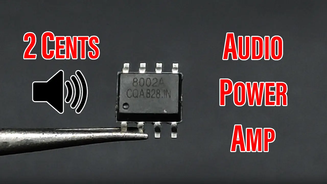
In this article, we’ll test the “2 Cents” 8002A audio power amplifier IC. I’ll follow its datasheet to build a simple audio amplifier circuit around that chip, prepare the files needed for manufacturing, and place the PCB SMT order at JLCPCB, who is kindly sponsoring this project.
Then, we’ll take some measurements for this audio power amplifier’s output power, distortion (THD), and see how good or bad it can be for a 2-cent 2W audio power amp chip. Let’s get right into it!
This Project is Sponsored By JLCPCB
Table of Contents
- 8002A Audio Power Amplifier
- 8002A Audio Amplifier Schematic Design
- Placing PCBA Order @ JLCPCB
- Amplifier’s Output Power Measurement
- Amplifier’s Distortion (THD) Measurement
- Wrap Up
- 8002A Audio Power Amplifier PCB Project Video
8002A Audio Power Amplifier
The 8002A is a low-cost audio power amplifier chip that’s designed specifically for low-power and portable devices. It operates at 5v DC and is still capable of delivering up to 2W of power into a 4Ω load. This is only possible thanks to the BTL configuration (bridged-tied load), so it drives the output speaker terminals differentially to deliver higher peak-to-peak voltage across the speaker terminals while working off a single voltage supply of 5v DC.
The technical specifications for the 8002A audio amplifier chip, as stated in the datasheet, are as follows:
- Operating Voltage: 2.2V up to 5.5V
- At 5V, less than 10% THD, it delivers:
- 1.5W into an 8Ω load
- 2W into a 4Ω load
- Shutdown mode (draws 4µA)
- Click & Pop Filtering/Protection during ON/OFF
- Low BOM cost (no output cap, bootstrap, snubber, filtering is needed)
- Unity gain stable + externally controllable gain
8002A Datasheet PDF
There are many variants of this audio power amplifier IC from different vendors, most of which are Chinese. However, here is an English version of the datasheet. Nevertheless, you should always take the values in the datasheet with a pinch of salt, as they may vary from one vendor to another.
8002A Audio Amplifier Schematic Design
The typical application circuit schematic mentioned in the datasheet is shown below. And this is exactly what I’m going to use in my PCB project. I’ll just change the feedback resistor (Rf) with a 50kΩ potentiometer to have a controllable gain.

Here is the PCB layout for the above circuit in KiCAD before exporting the fabrication gerber files.

Placing PCBA Order @ JLCPCB
Finally, we’re ready to generate the fabrication files and send them to JLCPCB for PCB fabrication and assembly. For this task, I use the KiCAD plugin named “Fabrication Toolkit”. With just one button click, you’ll have all manufacturing output files ready in a new folder that’s automatically created for you by the plugin toolkit.

1. Upload Your Gerber File & Check PCB Fab. Options
The next step is to upload your PCB Gerber files and modify the PCB fabrication options as needed in your project. Just keep an eye on the price because some options are not considered as a standard fabrication process, which will end up costing you a bit more and take a bit more time to get fabricated.
Even if you’re 100% sure that your design & fabrication files are flawless, the online system & JLCPCB or any other fab house can still pick up incorrect components’ orientation or placement. Always double-check the PCB component placement after uploading your files.
2. Upload BOM & CPL Files
The next step is to upload your design’s BOM file and the components positions file (CPL) to JLCPCB and let it check the files and report the stock status and total number of components to be assembled, their cost, and so on.

Check everything and make sure the components are selected correctly from the JLCPCB SMT library. And also double-check the component placements on the next page and correct any wrong rotations in the CPL file. There is a mismatch between the KiCAD output position file & JLCPCB’s system, so it does pick up wrong orientations for some ICs, diodes, etc. Always double-check everything before placing the order.
3. Pay To Place Your Order
The last step to place your order is to pay for the invoice and you can apply any valid discount coupon at this step to reduce the cost.
4. Wait For Delivery & Prepare For Testing!
You should expect to receive your board within 4 days to 1 week, depending on where you live.
Here is how it turned out at the end.

Amplifier’s Output Power Measurement
To test the 8002A audio power amplifier, I’ve used a signal generator 1kHz sine wave, a 4Ω dummy load, and my DSO oscilloscope to observe the output waveform and take the (peak-to-peak & RMS) voltage measurements to calculate the output power.
For the full testing procedure, please check my YouTube video regarding this project. But here is what I’ve got by conducting this test:
By increasing the input signal’s amplitude, I’ve managed to get an output peak-peak voltage of 4.5V just before clipping, barely getting into clipping.

Using our Audio Power Calculator tool, we’ll find out that the output power of this amplifier is around 0.6W of “clean sound”. Increasing the output power is possible, but at the cost of degraded sound quality (higher THD).
After going into clipping, the waveform is no longer sinusoidal, and you must not use the peak-to-peak voltage for power calculation. Instead, you should be using the Vrms measurement to find out the actual output power going into your load.
Even after clipping at 10% THD, which is awful, I still got an output Vrms of 1.77V into my 4Ω dummy load. Which is 0.8W, way behind the claimed “2W” output power stated in the datasheet.
Amplifier’s Distortion (THD) Measurement
To conduct this test, I’ve used my USB sound card for more accurate results. However, any scope FFT mode should be sufficient to measure 1% ~ 10% THD, like this amplifier is expected to be.
To get the cleanest output possible from this amplifier chip, I’ve set the input level in such a way that the output waveform is a bit lower than the clipping point of the amplifier.
The result was an output Vpp of 4.3V, which means the output power was 0.58W. And the THD measurement result was as shown below.

The THD measurement was -48dB, which in other words is a 0.4% THD.
Wrap Up
For a 2-cent audio power amplifier chip, the results are impressive. But given what was actually stated in the datasheet, it’s disappointing to see these numbers in an actual test scenario. However, for a small portable device, 0.6W of “clean audio” output using only a 5V source is pretty decent.
There you have it! If you’ve got any questions, suggestions, or things you’d like me to test regarding this project or any other one, please do not hesitate to leave me a comment below or on the YouTube channel’s video.