| Previous Tutorial | Tutorial 41 | Next Tutorial | |||||
| STM32 SPI Communication Tutorial | |||||||
| STM32 Course Home Page ???? | |||||||
In this tutorial, we’ll be discussing the SPI hardware in STM32 microcontrollers. Starting with an introduction to the Serial Peripheral Interface (SPI) communication. And we’ll get a closer look at the STM32 SPI hardware module and its internal functionalities, modes of operation, options, and configurations. In conclusion, we’ll take a look at the possible interrupt signals that can be triggered by the SPI hardware. And the different modes to perform SPI transmit & receive operations like (polling – interrupt – DMA).
Finally, we’ll check the available SPI configuration inside of CubeMX and how to configure & operate the peripheral using the provided HAL APIs. And that’s it for this theoretical tutorial. Next, we’ll do a couple of LABs to practice using SPI in different projects for communication and modules interfacing with STM32 microcontrollers.
[toc]
1. Introduction To SPI Communication
SPI is an acronym for (Serial Peripheral Interface) pronounced as “S-P-I” or “Spy”. Which is an interface bus typically used for serial communication between microcomputer systems and other devices, memories, and sensors. Usually used to interface Flash Memories, ADC, DAC, RTC, LCD, SDcards, and much more. The SPI was originally developed by Motorola back in the 80s to provide full-duplex serial communication to be used in embedded systems applications.
SPI Pin Conventions & Connections
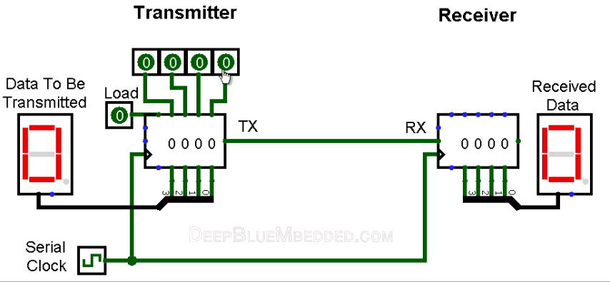
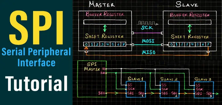
In typical SPI communication, there should be at least 2 devices attached to the SPI bus. One of them should be the master and the other will essentially be a slave. The master initiates communication by generating a serial clock signal to shift a data frame out, at the same time serial data is being shifted-in to the master. This process is the same whether it’s a read or write operation.
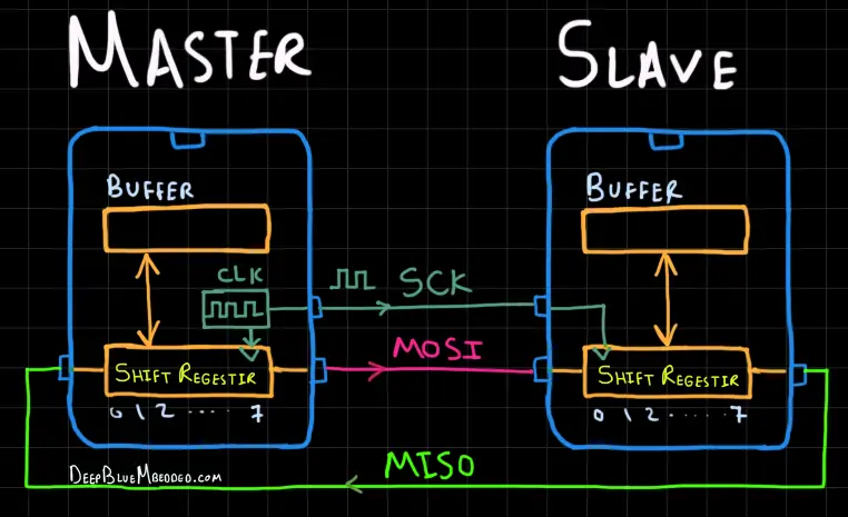
- MOSI -> Master output slave input (DOUT From Master).
- MISO -> Master input slave output (DOUT From Slave).
- SCLK -> Serial Clock, generated by the master and goes to the slave.
- SS -> Slave Select. Generated by the master to control which slave to talk to. It’s usually an active-low signal.
SPI Modes of Operation
Devices on the SPI bus can operate in either mode of the following: Master or Slave. There must be at least one master who initiates the serial communication process (For Reading/Writing). On the other hand, there can be single or multiple devices operating in slave mode.
The master device can select which slave to talk to by setting the SS (slave select) pin to logic low. If a single slave is being addressed, you can tie the SS pin of this slave device to logic low without the need to control this line by the master.
SPI Clock Configurations
The master SPI device is responsible for generating the clock signal to initiate and continue the data transaction process. The master, therefore, determines the data rate by controlling the serial clock line’s (SCK) frequency which is a programmable parameter in hardware by firmware instructions.
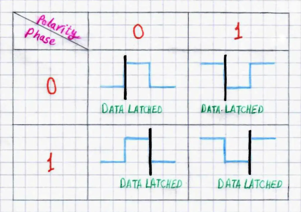
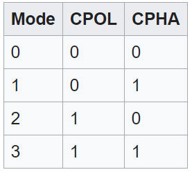
The SPI clock has two more parameters to control which are the Clock Phase (CPHA) and the Clock Polarity (CPOL). The clock phase determines the phase at which the data latching occurs at each bit transfer whether it’s the leading edge or the trailing edge. The clock polarity determines the IDLE state of the clock line whether it’s a HIGH or LOW. Having 2 possible states for each of the CPOL and CPHA gives us a total of 4 possible modes for the SPI clock. Typically referred to as “SPI Mode Number”.
 |
 |
| Check this in-depth tutorial for more information about SPI serial communication | |
 |
 |
The linked SPI tutorial above is a full guide (+8k words!) that has all the information you may need to know if you’re just starting to learn about the topic. Take the time to check it out if you need to and come back to resume this tutorial and to see the SPI hardware peripheral implemented in STM32 microcontrollers and the extra features it does have.
2. SPI Hardware In STM32
2.1 STM32 SPI Hardware Overview
the STM32 SPI interface provides two main functions, supporting either the SPI protocol or the I2S audio protocol. By default, it is the SPI function that is selected. It is possible to switch the interface from SPI to I2S by software.
The serial peripheral interface (SPI) allows half/ full-duplex, synchronous, serial communication with external devices. The interface can be configured as the master and in this case, it provides the communication clock (SCK) to the external slave device. The interface is also capable of operating in a multi-master configuration.
2.2 STM32 SPI Main Features
- Full-duplex synchronous transfers on three lines
- Simplex synchronous transfers on two lines with or without a bidirectional data line
- 8- or 16-bit transfer frame format selection
- Master or slave operation
- Multimaster mode capability
- 8 master mode baud rate prescalers (fPCLK/2 max.)
- Slave mode frequency (fPCLK/2 max)
- NSS pin management by hardware or software for both master and slave: dynamic change of master/slave operations
- Programmable clock polarity and phase
- Programmable data order with MSB-first or LSB-first shifting
- Dedicated transmission and reception flags with interrupt capability
- SPI bus busy status flag
- Hardware CRC feature for reliable communication: [ CRC value can be transmitted as the last byte in Tx mode – Automatic CRC error checking for last received byte ]
- Master mode fault, overrun, and CRC error flags with interrupt capability
- 1-byte transmission and reception buffer with DMA capability: Tx and Rx requests
3. STM32 SPI Hardware Functionalities
In this section, we’ll get a deep insight into the STM32 SPI module hardware, its block diagram, functionalities, modes of operations, and data reception/transmission.
3.1 STM32 SPI Block Diagram
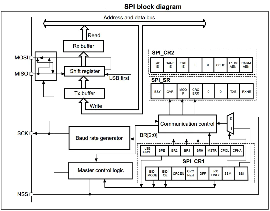
As you can see in the SPI block diagram above, there is the main shift register lying between two buffer registers one for transmission (TX) and the other for reception (RX). And a logical control unit on the right side with a bunch of signals coming in and out to the control registers.
The control registers give you the ability to change any of the SPI hardware configurations by software instructions. And there is also the status register that gives you some signals about the ongoing and last-done transaction and any error if happened.
The baud rate generator (Clock signal SCK) is also configurable by software as we can tell and there is a control logic dedicated for the NSS pin (if you’re going to use it).
3.2 STM32 SPI Data Frame Format
Data can be shifted out either MSB-first or LSB-first depending on the value of the LSBFIRST bit in the SPI_CR1 Register.
Each data frame is 8 or 16 bits long depending on the size of the data programmed using the DFF bit in the SPI_CR1 register. The selected data frame format is applicable for transmission and/or reception.
It has to be the same on both ends of the communication. The slave should know what to expect in order to read the received data correctly. It has to be formatted coordinately.
3.3 STM32 SPI In Slave Mode
In the slave configuration, the serial clock is received on the SCK pin from the master device. The baud rate value set in the BR[2:0] bits in the SPI_CR1 register, does not affect the data transfer rate. In this configuration, the MOSI pin is a data input pin and the MISO pin is a data output.
Note that you need to have the SPI slave device running and configured before the master starts to send anything just to avoid any possible data corruption at the beginning of the first communication session.
The configuration procedure is available in the datasheet if you’d like to follow it in order to build an SPI initialization function at the register-level. But we’ll be using the HAL APIs so it’ll handle this procedure for us regardless of the specific STM32 target microcontroller we’re using in the design.
Transmit Sequence in Slave Mode
The data byte is parallel-loaded into the Tx buffer during a write cycle. The transmit sequence begins when the slave device receives the clock signal and the most significant bit of the data on its MOSI pin. The remaining bits (the 7 bits in 8-bit data frame format, and the 15 bits in 16-bit data frame format) are loaded into the shift-register. The TXE flag in the SPI_SR register is set on the transfer of data from the Tx Buffer to the shift register and an interrupt is generated if the TXEIE bit in the SPI_CR2 register is set.
Receive Sequence in Slave Mode
For the receiver, when data transfer is complete: The Data in the shift register is transferred to Rx Buffer and the RXNE flag (SPI_SR register) is set. An Interrupt is generated if the RXNEIE bit is set in the SPI_CR2 register.
After the last sampling clock edge, the RXNE bit is set, a copy of the data byte received in the shift register is moved to the Rx buffer. When the SPI_DR register is read, the SPI peripheral returns this buffered value. Clearing of the RXNE bit is performed by reading the SPI_DR register.
3.4 STM32 SPI In Master Mode
In the master configuration, the serial clock is generated on the SCK pin. In this configuration, the MOSI pin is a data output pin and the MISO pin is data input.
Transmit Sequence in Master Mode
The transmit sequence begins when a byte is written in the Tx Buffer. The data byte is parallel-loaded into the shift register (from the internal bus) during the first-bit transmission and then shifted out serially to the MOSI pin MSB first or LSB first depending on the LSBFIRST bit in the SPI_CR1 register.
The TXE flag is set on the transfer of data from the Tx Buffer to the shift register and an interrupt is generated if the TXEIE bit in the SPI_CR2 register is set.
Receive Sequence in Master Mode
For the receiver, when data transfer is complete: The data in the shift register is transferred to the RX Buffer and the RXNE flag is set. An interrupt is generated if the RXNEIE bit is set in the SPI_CR2 register
At the last sampling clock edge, the RXNE bit is set, a copy of the data byte received in the shift register is moved to the Rx buffer. When the SPI_DR register is read, the SPI peripheral returns this buffered value.
Clearing the RXNE bit is performed by reading the SPI_DR register. A continuous transmit stream can be maintained if the next data to be transmitted is put in the Tx buffer once the transmission is started. Note that the TXE flag should be ‘1 before any attempt to write the Tx buffer is made.
3.5 SPI Half-Duplex Communication Configuration
The STM32 SPI Hardware is capable of operating in half-duplex mode in 2 configurations.
- 1 clock and 1 bidirectional data wire
- 1 clock and 1 data wire (receive-only or transmit-only)
Check the target MCU’s datasheet for more information about each configuration of them if you’re going to use this Half-Duplex mode. I don’t think we’d need that in any of the future tutorials. But if we did, I’ll give some examples to do this type of communication with SPI.
3.6 STM32 SPI Data Transmission & Reception
In reception, data are received and then stored into an internal Rx buffer while In transmission, data are first stored into an internal Tx buffer before being transmitted.
A read access to the SPI_DR register returns the Rx buffered value, whereas a write access to the SPI_DR stores the written data into the Tx buffer.
3.6 STM32 SPI CRC Calculation
A CRC calculator has been implemented in STM32 SPI hardware for communication reliability. Separate CRC calculators are implemented for transmitted data and received data. The CRC is calculated using a programmable polynomial serially on each bit. It is calculated on the sampling clock edge defined by the CPHA and CPOL bits in the SPI_CR1 register.
At the end of data and CRC transfers, the CRCERR flag in the SPI_SR register is set if corruption occurs during the transfer. This is similar to a checksum if you’re familiar with error detection procedures for communication. Actually, the checksum is a very simple way of doing a mathematical operation (addition) to the data being transferred to check the validity of the whole data packet.
The CRC (cyclic redundancy check) is a much “mathematically” powerful operation than a normal checksum that’s much harder to fool. There are many different versions and equations for performing CRC in general but it’s really good to have it built within the SPI hardware itself.
4. STM32 SPI Flags (Status & Errors)
There are some status flags provided for the application to completely monitor the state of the SPI bus.
- Tx buffer empty flag (TXE) – When it is set, this flag indicates that the Tx buffer is empty and the next data to be transmitted can be loaded into the buffer. The TXE flag is cleared when writing to the SPI_DR register.
- Rx buffer not empty (RXNE) – When set, this flag indicates that there are valid received data in the Rx buffer. It is cleared when SPI_DR is read.
- BUSY flag – The BSY flag is useful to detect the end of a transfer if the software wants to disable the SPI and enter Halt mode (or disable the peripheral clock). This avoids corrupting the last transfer. For this, the procedure described below must be strictly respected. The BSY flag is also useful to avoid write collisions in a multi-master system.
There are also other SPI flags that indicate whether a specific type of error has occurred or not.
- SPI Master mode fault (MODF) – Master mode fault occurs when the master device has its NSS pin pulled low (in NSS hardware mode) or SSI bit low (in NSS software mode), this automatically sets the MODF bit.
- SPI Overrun condition – An overrun condition occurs when the master device has sent data bytes and the slave device has not cleared the RXNE bit resulting from the previous data byte transmitted.
- SPI CRC error – This flag is used to verify the validity of the value received when the CRCEN bit in the SPI_CR1 register is set. The CRCERR flag in the SPI_SR register is set if the value received in the shift register does not match the receiver SPI_RXCRCR value.
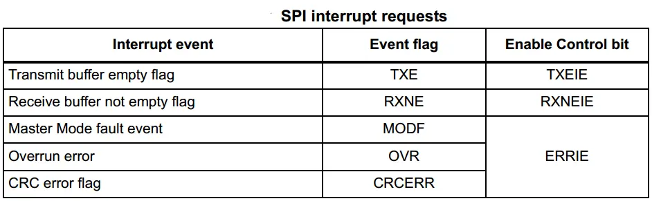
5. STM32 SPI Interrupts
The SPI interrupt events are connected to the same interrupt vector. So the SPI fires a single interrupt signal regardless of the source of it. The software will have to detect it. These events generate an interrupt if the corresponding Enable Control Bit is set.
6. STM32 SPI Transmit & Receive Modes
In this section, I’ll list the possible ways that you can handle SPI transactions in your firmware applications. For code example LABs and testing, just click on the next tutorial button and keep going through this series of tutorials. There will be lots of examples and libraries that we’ll build based on SPI communication.
SPI With Polling
The first and the easiest way to do anything in embedded software is just to poll for the hardware resource until it’s ready to move on to the next step in your program instructions. However, it’s the least efficient way to do things and the CPU will end up wasting so much time in a “busy-waiting” state.
It’s the same thing for both transmission and reception. You just wait until the current byte of data to be transmitted so you can start the next one and so on.
SPI With Interrupts
We can, however, enable the SPI interrupts and have a signal when it’s done and ready for servicing by CPU. Either for data that has been sent or received. Which saves a lot of time and has been always the best way to handle events like that.
However, in some “Time Critical” applications we need everything to be as deterministic, in time, as possible. And a major problem with interrupts is that we can’t expect when it’d arrive or during which task. That can potentially screw up the timing behavior of the system, Especially with an extremely fast communication bus like SPI that can definitely block the CPU if you’re receiving massive data blocks at a very high rate.
SPI With DMA
To operate at its maximum speed, the SPI needs to be fed with the data for transmission and the data received on the Rx buffer should be read to avoid overrun. To facilitate the transfers, the SPI features a DMA capability implementing a simple request/acknowledge protocol.
A DMA access is requested when the enable bit in the SPI_CR2 register is enabled. Separate requests must be issued to the Tx and Rx buffers.
Using the DMA unit not only will make the SPI going at full speed on both sides of communication, but it will also free the CPU from doing the data transfers “from peripheral to memory”. This will end up saving a lot of time and is considered to be the most efficient way to handle this peripheral to memory data transfer and vice versa.
7. SPI Configuration In CubeMX
In the next few tutorials, we’ll be doing some practical LABs to implement SPI receiver/transmitter code examples. In which we’ll be using the CubeMX software tool to configure the SPI hardware. Therefore, in this section, I’ll introduce to you the features and options that can be configured within CubeMX GUI for SPI peripheral.
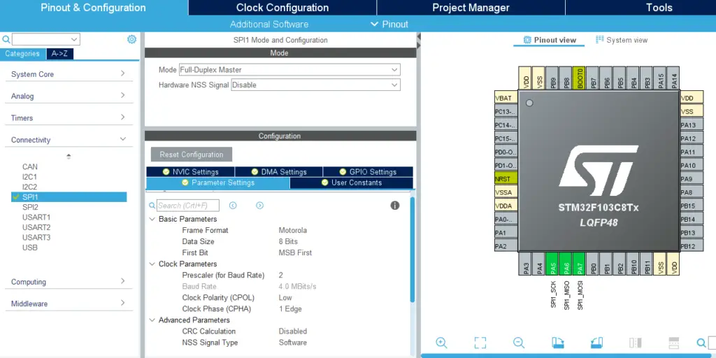
Here is the configuration tab for the SPI peripheral in CubeMX. And those are the possible modes for SPI.
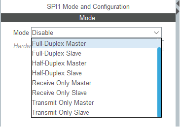
Let’s pick the “Full-Duplex Master” mode for example. You’ll find that now we’re able to set the baud rate, frame type and size, NSS pin control, CRC, SPI Mode Number (Clock Phase & Polarity), and other parameters.
We can also enable/disable interrupts for SPI in the NVIC tab if you’re willing to use interrupt mode instead of polling the peripheral. And the same goes for the DMA, you can click the DMA tab to “Add” a DMA channel dedicated to SPI transfer and configure its parameters.
8. SPI HAL Functions APIs
1. STM32 SPI Blocking Mode HAL Functions
For Transmission
|
1 |
HAL_SPI_Transmit(SPI_HandleTypeDef * hspi, uint8_t * pData, uint16_t Size, uint32_t Timeout); |
For Reception
|
1 |
HAL_SPI_Receive(SPI_HandleTypeDef * hspi, uint8_t * pData, uint16_t Size, uint32_t Timeout); |
For Transmit-Receive
|
1 |
HAL_SPI_TransmitReceive(SPI_HandleTypeDef * hspi, uint8_t * pTxData, uint8_t * pRxData, uint16_t Size, uint32_t Timeout); |
2. STM32 SPI Interrupt Mode HAL Functions
For Transmission
|
1 |
HAL_SPI_Transmit_IT(SPI_HandleTypeDef * hspi, uint8_t * pData, uint16_t Size); |
After calling the above function, the SPI peripheral will start sending all the data bytes in the buffer one by one until it’s done. When it’s done this function below will be called and executed, if you’d like to do something upon data transmission completion, then add that to your code in the application source file (main.c).
|
1 2 3 4 |
void HAL_SPI_TxCpltCallback(SPI_HandleTypeDef * hspi) { // TX Done .. Do Something ... } |
For Reception
|
1 |
HAL_SPI_Receive_IT(SPI_HandleTypeDef * hspi, uint8_t * pData, uint16_t Size); |
After calling the above function, the SPI peripheral will start receiving all the incoming data bytes in the buffer one by one until it’s done. When it’s done this function below will be called and executed, if you’d like to do something upon data reception completion, then add that to your code in the application source file (main.c).
|
1 2 3 4 |
void HAL_SPI_RxCpltCallback(SPI_HandleTypeDef * hspi) { // RX Done .. Do Something ... } |
For Transmit-Receive
|
1 |
HAL_SPI_TransmitReceive_IT(SPI_HandleTypeDef * hspi, uint8_t * pTxData, uint8_t * pRxData, uint16_t Size); |
After calling the above function, the SPI peripheral will start sending-receiving all the incoming data bytes in the buffers one by one until it’s done. When it’s done this function below will be called and executed, if you’d like to do something upon data transmission-reception completion, then add that to your code in the application source file (main.c).
|
1 2 3 4 |
void HAL_SPI_TxRxCpltCallback(SPI_HandleTypeDef * hspi) { // TX-RX Done .. Do Something ... } |
3. STM32 SPI DMA Mode HAL Functions
For Transmission
|
1 |
HAL_SPI_Transmit_DMA(SPI_HandleTypeDef * hspi, uint8_t * pData, uint16_t Size); |
After calling the above function, the SPI peripheral will start sending all the data bytes in the buffer one by one until it’s done (in DMA Mode). When it’s done this function below will be called and executed, if you’d like to do something upon data transmission completion, then add that to your code in the application source file (main.c).
|
1 2 3 4 |
void HAL_SPI_TxCpltCallback(SPI_HandleTypeDef * hspi) { // TX Done .. Do Something ... } |
For Reception
|
1 |
HAL_SPI_Receive_DMA(SPI_HandleTypeDef * hspi, uint8_t * pData, uint16_t Size); |
After calling the above function, the SPI peripheral will start receiving all the incoming data bytes in the buffer one by one until it’s done (in DMA Mode). When it’s done this function below will be called and executed, if you’d like to do something upon data reception completion, then add that to your code in the application source file (main.c).
|
1 2 3 4 |
void HAL_SPI_RxCpltCallback(SPI_HandleTypeDef * hspi) { // RX Done .. Do Something ... } |
For Transmit-Receive
|
1 |
HAL_SPI_TransmitReceive_DMA(SPI_HandleTypeDef * hspi, uint8_t * pTxData, uint8_t * pRxData, uint16_t Size); |
After calling the above function, the SPI peripheral will start sending-receiving all the incoming data bytes in the buffers one by one until it’s done (in DMA Mode). When it’s done this function below will be called and executed, if you’d like to do something upon data transmission-reception completion, then add that to your code in the application source file (main.c).
|
1 2 3 4 |
void HAL_SPI_TxRxCpltCallback(SPI_HandleTypeDef * hspi) { // TX-RX Done .. Do Something ... } |
The SPI Communication Bus Demonstrated in This Tutorial Will Be Used In The Following Next Tutorials:
- MCU – MCU Communication Over SPI
- External Serial SPI FLASH
- SD Card Interfacing
- Dot Matrix Display
- nRF24L01 Driver Library
- and more…
That’s it for this tutorial. If you’d like to see the practical LAB examples for SPI and other interfacing projects and libraries we’ll build using this peripheral, just keep progressing through this series of tutorials and click to the next tutorial link down below.
Did you find this helpful? If yes, please consider supporting this work and sharing these tutorials!
Stay tuned for the upcoming tutorials and don’t forget to SHARE these tutorials. And consider SUPPORTING this work to keep publishing free content just like this!
| Previous Tutorial | Tutorial 41 | Next Tutorial | |||||
Hi,
I am a student embedded hardware and i am having some problems with using the nRF24L01 in a project. I used a library i found online but it does not seem to work. In this tutorial i saw that you mentioned a tutorial about the nRF24L01 but i can’t find it on the site. Can you maybe help me understand how to work with the nRF24L01?
Many thanks!